4 Minutes
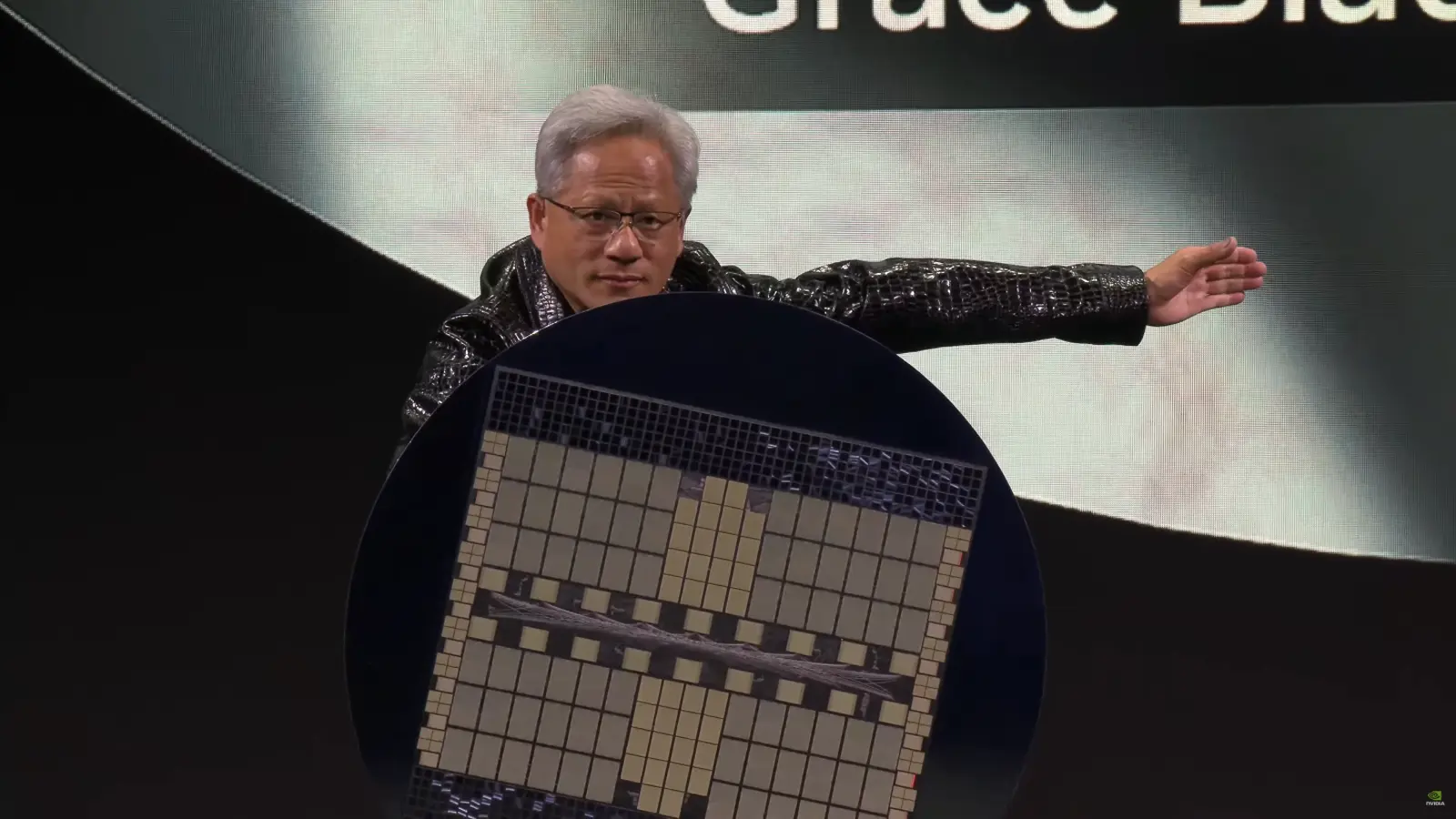
NVIDIA CEO Jensen Huang has confirmed that the company is actively preparing its next-generation Rubin AI architecture at TSMC. Described internally as a revolutionary step for compute, Rubin represents a ground-up redesign of NVIDIA’s data center stack — from memory and process node to packaging and interconnects. Huang revealed that NVIDIA has already taped out six Rubin chips that are now in TSMC’s fabs and being readied for trial production.
What Jensen Huang Announced
During his visit to Taiwan, Huang told local media that Rubin is “very advanced” and that six separate Rubin chips have been taped out and handed to TSMC. These include new CPU and GPU dies plus specialized silicon for scaling and connectivity. The announcement signals a broad platform refresh rather than an incremental update.
Chips Confirmed in Tape-Out
- Dedicated CPU die
- Next-generation GPU (expected R100 family)
- Scale-up NVLink Switch for higher-bandwidth multi-GPU scaling
- Silicon photonics processor for optical I/O
- Additional interposer/bridge dies to support chiplet integration
- Packaging and switch logic chips
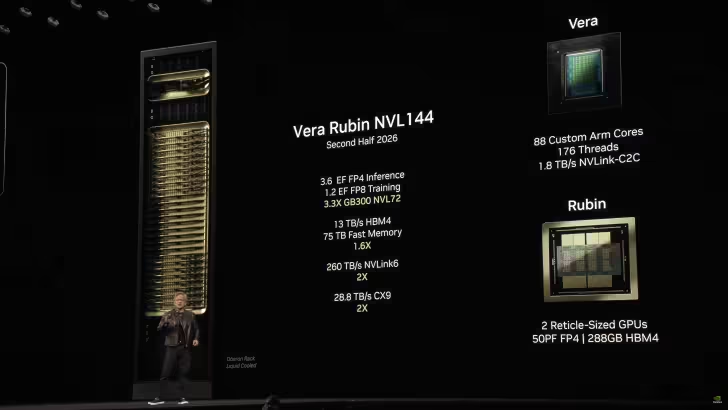
Technical Features and Innovations
Rubin packs several high-impact upgrades for AI compute. NVIDIA plans to use HBM4 memory to power R100 GPUs, a significant move beyond the current HBM3E standard. The design will leverage TSMC’s 3nm-class N3P process and CoWoS-L advanced packaging. Crucially, Rubin adopts a chiplet architecture — a first for NVIDIA at this scale — and moves to a 4x reticle layout versus Blackwell’s ~3.3x reticle, enabling larger combined die areas and more modular scaling. The inclusion of a silicon photonics processor and a scale-up NVLink Switch underscores a focus on high-bandwidth, low-latency interconnect for distributed AI workloads.
Comparisons: Rubin vs Blackwell and Hopper
Where Blackwell Ultra (GB300) represented a near-term peak in NVIDIA’s current roadmap, Rubin aims to be a generational leap comparable to what Hopper delivered earlier. Rubin’s shift to chiplets, HBM4, N3P, and CoWoS-L packaging suggests performance, power efficiency, and scaling improvements across training and inference workloads. The architectural changes are deeper than a simple process-node refresh — they touch memory architecture, physical packaging, and interconnect topology.
Advantages and Use Cases
Rubin is optimized for large-scale AI training, massive language models, and high-performance computing where memory bandwidth and inter-node communication are limiting factors. Silicon photonics and a scale-up NVLink Switch make Rubin compelling for hyperscalers and enterprise AI clusters that demand dense, low-latency fabric. The chiplet approach could also improve yield and accelerate time-to-market for different SKUs aimed at training, inference, and edge-accelerated servers.
Market Relevance and Timeline
Given tape-out and TSMC trial production underway, Rubin’s commercial debut is tentatively expected in the 2026–2027 window, depending on qualification and yield ramp. For cloud providers, OEMs, and AI infrastructure vendors, Rubin represents a strategic node: it could reset performance baselines in the AI server market and drive new rounds of hardware refreshes across data centers.
Conclusion
NVIDIA’s Rubin appears poised to be a watershed architecture: combining HBM4 memory, TSMC’s 3nm process, chiplet modularity, CoWoS-L packaging, and optical I/O to deliver a next-level platform for AI and HPC. With six tape-outs already at TSMC, the industry will be watching trial production closely as Rubin moves toward a likely 2026–2027 launch.
Source: wccftech
Leave a Comment