3 Minutes
The Battle for Advanced Semiconductor Manufacturing
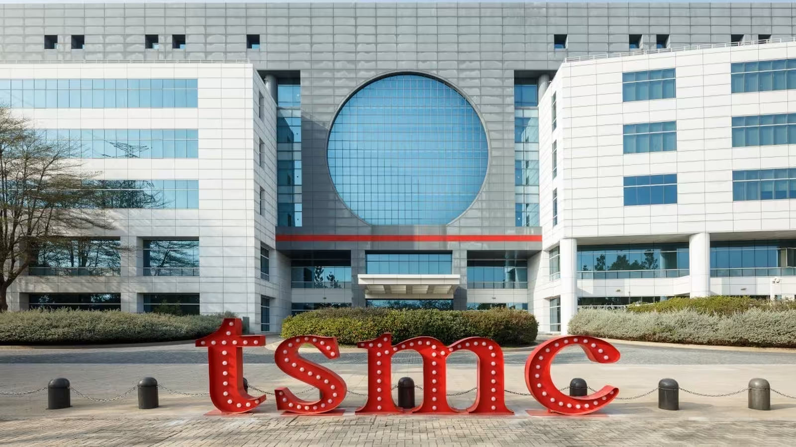
For companies designing next-generation consumer electronics, AI processors, and flagship smartphones, the choice of semiconductor foundry can make or break product success. As the demand for advanced 3nm chips heats up, the global market has become a fierce battleground between foundry giants TSMC and Samsung Foundry.
Why TSMC Is the First Choice for 3nm Chips
Fabless chipmakers — those companies that design chips but lack manufacturing plants, such as Apple, Nvidia, and Qualcomm — have just two primary options for fabricating top-tier semiconductors: Taiwan’s TSMC or South Korea’s Samsung Foundry. However, when it comes to 3nm process nodes, TSMC dominates the field.
Advanced nodes like 3nm are prized for their ability to deliver higher performance and energy efficiency in CPUs, GPUs, and SoCs. Yet manufacturing at this scale is technically complex and demands a high yield — the percentage of working chips from a production batch. TSMC currently boasts a yield rate above 90% for its 3nm process, while Samsung reportedly lags behind at around 50%. The clear yield advantage positions TSMC as the preferred—and often only—viable choice, even if it comes at a premium or with capacity constraints.
Customer Loyalty and Market Impact
Leading technology firms underline TSMC’s trusted reputation. Apple, MediaTek, and Nvidia are among its flagship customers. Qualcomm, too, made headlines when it switched production of its Snapdragon 8 Gen 1 away from Samsung Foundry due to disappointing yield rates, opting for a more reliable partnership with TSMC for subsequent chipsets.
Notable Features of TSMC’s 3nm Process
- Industry-leading yield rates exceeding 90%
- Ability to pack billions of transistors in a compact node
- Greater power efficiency and performance for mobile devices and AI hardware
Competition: Samsung and SMIC in the Global Race
While TSMC leads the 3nm segment, Samsung Foundry remains a distant second and faces further pressure from emerging competitors like China’s SMIC. As the world’s third-largest foundry, SMIC has made significant progress despite global trade restrictions that prevent access to cutting-edge extreme ultraviolet lithography (EUV) technology from American and Dutch suppliers.
To circumvent these barriers, SMIC utilizes older Deep Ultraviolet Lithography (DUV) machines, acquired before sanctions took force, to produce advanced chips such as Huawei’s 5nm Kirin X90 for the Mate Book Pro. This workaround, which requires multiple patterning steps, increases production complexity and costs—but enables continued progress for China’s tech sector.
Expanding Use Cases and Market Shifts
SMIC is now pivoting towards supplying 5nm and 7nm chips for China's automotive industry—a sector that has largely relied on Samsung Foundry. Continued advances from SMIC could further erode Samsung’s market share, especially as domestic demand in China grows.
The Future: 2nm Process and Beyond
Looking ahead, the race for ever-smaller semiconductor nodes continues. TSMC plans to introduce ultra-advanced 2nm chips as soon as next year, debuting in flagship devices like Apple’s iPhone 17 series. With unrivaled process technology and a strong customer base, TSMC is positioned to extend its dominance in advanced semiconductor manufacturing well beyond 2026.
Conclusion: The Importance of Foundry Choice
As the global tech landscape evolves, the reliability, efficiency, and performance of semiconductor manufacturing remain critical. For now, TSMC’s leadership in 3nm wafer production secures its place at the top, while rivals scramble to catch up in a fierce, ever-advancing industry.
Comments