3 Minutes
Huawei Embarks on Advanced 3nm Chip Development
Huawei is pushing the boundaries of chip manufacturing as it embarks on the ambitious journey to develop two state-of-the-art 3nm chips. Despite enduring strict US trade sanctions that block access to the latest semiconductor technologies, the Chinese tech giant is determined to advance its semiconductor capabilities, signaling a significant shift in the global chip industry.
Dual-Track Strategy: GAA FET and Carbon Nanotubes
Leaks from industry insiders and Taiwanese media have revealed that Huawei is pursuing a dynamic dual-track approach. The first path focuses on a 3nm Gate-All-Around (GAA) FET-based chip, a next-generation transistor design known for boosting power efficiency and performance in processors. The second, even more groundbreaking, involves pioneering semiconductors based on carbon nanotube (CNT) technology—a potential leap beyond traditional silicon chips. Both designs are targeting a tape-out milestone by 2026, with mass production possibly commencing as soon as 2027 if technical progress continues smoothly.
Building on Past Success and Overcoming Technological Barriers
Huawei’s strategy draws heavily from recent achievements, such as the 5nm Kirin X90, manufactured by SMIC without access to advanced EUV lithography equipment from ASML. By utilizing Deep Ultraviolet (DUV) lithography and intricate multi-patterning techniques, SMIC achieved the production of these chips, albeit with lower yields—about 20%—compared to industry leaders like TSMC and Samsung, who use Extreme Ultraviolet (EUV) lithography for their 3nm processes.
While GAA FET chips can potentially deliver superior performance and energy savings compared to previous Kirin generations, the innovation with carbon nanotubes holds the promise of surpassing traditional silicon’s limitations, though commercial viability remains uncertain.
Challenges, Competition, and the Future of the Semiconductor Race
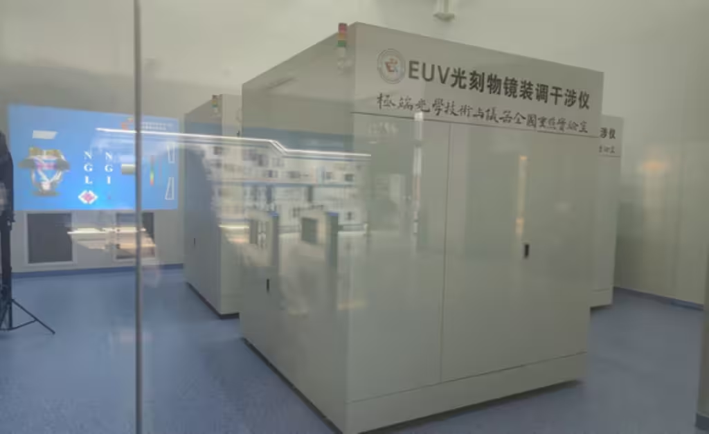
The primary challenge lies in yield rates, which could drop even further at the tiny 3nm scale due to the constraints of DUV technology—increasing production costs and complexity. However, Huawei is heavily investing—over $37 billion—in the domestic development of its own EUV lithography tools. Some experts and industry observers express optimism that Huawei could achieve key EUV breakthroughs by 2026, potentially reducing its reliance on international suppliers. Still, skepticism remains, as established players like ASML have long dominated in EUV technology.
Market Impact and Global Significance
Should Huawei succeed in delivering competitive 3nm chips using GAA FET and potentially carbon nanotube architectures, it could significantly narrow the gap with semiconductor giants TSMC and Samsung. This would not only elevate China’s position in the global chip race but could also spur innovation and competition industry-wide. Still, persistent hurdles—like low yields and dependence on DUV—must be overcome.
As 2026 approaches, the tech world will closely watch for further developments and potential breakthroughs in Huawei’s chip ambitions, which could transform the semiconductor landscape on a global scale.
Comments