3 Minutes
TSMC 2nm Mass Production Set for Q4
Following earlier reports of yield challenges, Taiwan Semiconductor Manufacturing Company (TSMC) appears to have stabilized its 2nm (N2) process and is now targeting mass production in Q4 of this year, according to DigiTimes. The renewed ramp signals a major milestone for semiconductor manufacturing, with the foundry planning parallel production at its Baoshan and Kaohsiung fabs.
Production Ramp and Capacity
Fab locations and wafer output
TSMC will reportedly start simultaneous volume production at both Baoshan and Kaohsiung, aiming for a combined monthly wafer output of roughly 45,000–50,000 units by the end of the year. That capacity is projected to roughly double in 2026 as the company completes additional tooling and process tuning.
Customers, Roadmap and Market Impact
Initial customers and order allocations
Early customers slated to receive N2 node wafers include Apple, AMD, Qualcomm, MediaTek, Broadcom and Intel. Cupertino is said to have secured about half of the initial order book. Nvidia is expected to begin consuming 2nm silicon in 2027 as production capacity expands, particularly for high-performance compute and AI accelerators.
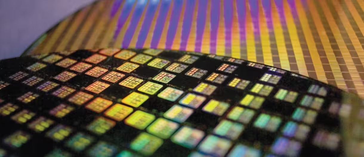
Product Features and Technical Advantages
Performance, power and density
The 2nm (N2) process promises improved transistor density and better performance-per-watt compared with TSMC’s 3nm node. Early rumor projections indicate roughly 10–15% raw performance gains for Apple’s upcoming A19 chip compared with its 3nm predecessors, alongside power-efficiency improvements that benefit both mobile SoCs and data-center accelerators.
Comparisons and Use Cases
Compared with 3nm, the N2 node targets higher clock ceilings, reduced power draw at the same performance, and increased transistor density for more complex SoC architectures. Primary use cases include flagship smartphone SoCs (e.g., Apple A19 for the iPhone 18 series), high-performance CPUs and GPUs from AMD and Intel, network and connectivity silicon from Broadcom and MediaTek, and future Nvidia AI chips.
Advantages for the Industry
A stabilized 2nm ramp reduces risk of customer delays, shortens time-to-market for next-gen devices, and strengthens TSMC’s leadership in advanced semiconductor manufacturing. For OEMs and cloud providers, broader access to N2 capacity will accelerate innovation in AI, mobile, and edge computing.
Outlook
Assuming TSMC meets the Q4 target and scales as planned in 2026–2027, the industry should see a steady trickle of 2nm-based products from mobile devices to datacenter accelerators over the next 18–36 months. Continued monitoring of yield trends and customer adoption will determine how quickly the node becomes mainstream across segments.
Source: gsmarena
Leave a Comment