
Numbers that once meant something now feel like product slogans. Short. Memorable. Misleading.
When IBM unveiled its so-called 0.7‑nanometer process, the announcement read like a technological milestone: denser transistors, vertical stacking via nanostacking, and wafer bonding to glue silicon layers together. Engineers described transistors built one on top of another to squeeze more switching elements into the same footprint. It sounds like progress. It also sounds like a marketing line.
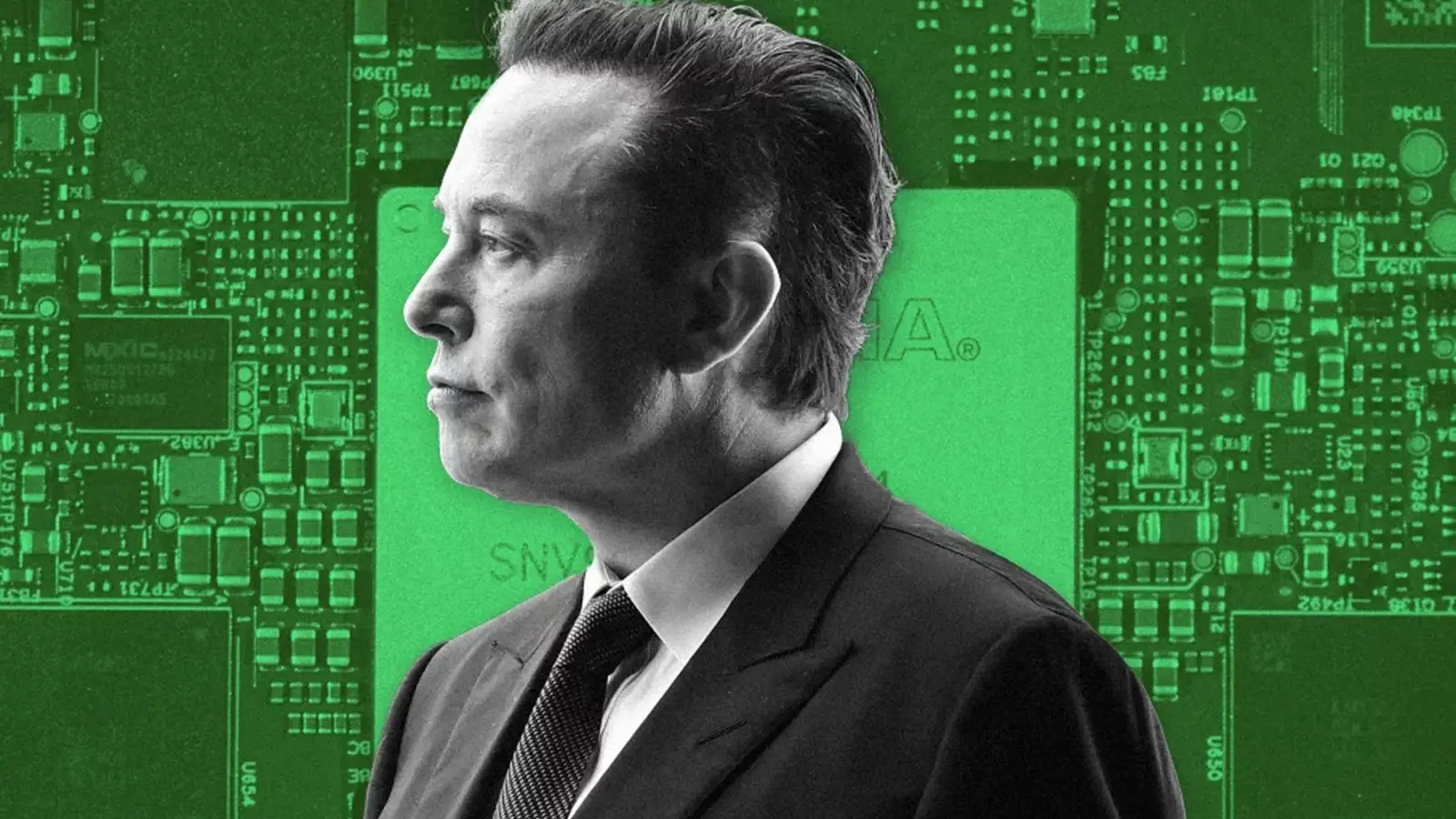
Enter Elon Musk. On X, he pushed back and suggested a different yardstick: count the atoms. Musk's point was simple and stinging — if a label like "0.7nm" doesn’t correspond to a physically meaningful dimension in the chip’s critical structures, why keep using it? He argued that the number of atoms in the smallest transistor features would be a far more honest, intrinsic metric.
IBM itself admitted something similar in its blog post: the "0.7nm" tag is effectively a brand for this generation of technology. Decades ago, process names roughly matched gate lengths or metal pitches. Today, with multi‑patterning, stacked transistors and heterogeneous materials, those labels no longer map cleanly to any single physical measure. The industry evolved; the naming conventions didn’t keep pace.

That discrepancy isn’t new. Intel rewrote its roadmap names in 2021, renaming a 10nm lineage to Intel 7 and a later node to Intel 4. TSMC, meanwhile, continued using its own commercial names as it ramped capacity and fed partners like AMD. The result is a marketplace where "nm" often signals marketing position and performance class, not an atomic ruler.
Could atom counting fix this? In principle, counting atoms is a blunt way to show size at the ultimate limit. In practice, it’s messy. Chips are three‑dimensional now. Materials differ. A gate made from one compound may need a different atomic spacing than another. Are we counting atoms along one axis? Across a gate? Including spacer atoms? The methodology would have to be standardized. That’s not impossible, but it is complicated.
More to the point: transparency matters. Engineers, customers and regulators all benefit when vendors clarify what their labels mean — whether that’s transistor density, effective channel length, contact pitch, or a bundled performance and power expectation. Marketing language alone corrodes trust. That’s the heart of Musk’s gripe.
This debate is also a signpost for the industry’s next phase. Shrinking a single planar dimension isn’t the only lever anymore. Stacking, new device architectures, advanced materials and packaging innovations are the levers that actually drive real gains. So maybe chip names should tell a story: what changed, and how users will feel the difference in performance, efficiency or cost.
Transparent metrics. Agreed definitions. Less theater. The industry can keep its bravado — but only if the numbers start meaning what everyone assumes they do.
.avif "China Debuts Homegrown E-Beam Lithography 'Xizhi' — A Strategic Step Toward Domestic Chipmaking")

Leave a Comment
Comments
No comments yet. Be the first.