.avif)
6 Minutes
China rolls out its first domestically produced e-beam lithography system
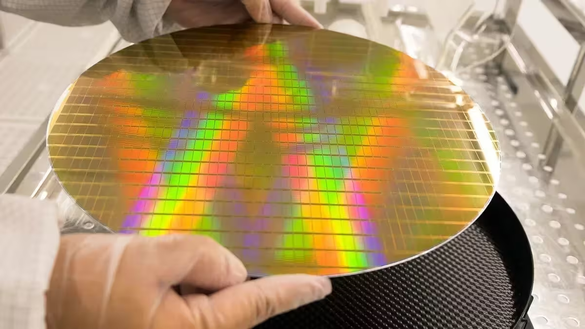
China has announced the delivery of its first homegrown electron-beam (e-beam) lithography system, named Xizhi, developed at Zhejiang University in Hangzhou. The milestone comes amid persistent export controls that have blocked the most advanced Extreme Ultraviolet (EUV) lithography systems — produced largely by the Dutch company ASML — from being exported to China. While Deep Ultraviolet (DUV) lithography systems continue to be available at a lower technology tier, the arrival of Xizhi represents a meaningful step in China’s push to build an independent semiconductor equipment ecosystem.
Why lithography matters: nodes, wavelengths and transistor density
At the heart of modern chip manufacturing is lithography: the process used to transfer circuit patterns onto silicon wafers. Different lithography technologies use different wavelengths (or beams) to create finer features. DUV systems typically work with 193 nm light, while EUV operates at a much shorter 13.5 nm wavelength — enabling patterning for process nodes below 7 nm. Smaller process nodes and higher transistor density (measured in millions or billions of transistors per square millimeter) enable chips to be more powerful and energy-efficient. Leading foundries such as TSMC and Samsung are scaling into 2 nm-class nodes, underscoring the gap China faces without ready access to top-tier EUV tools.
What Xizhi is and what it delivers
Xizhi is an e-beam lithography tool that uses focused electron beams to write circuit patterns directly onto wafers or masks. According to local reports, the system can achieve line widths down to about 8 nm and claims a positioning accuracy of roughly 0.6 nm — specifications that align with international research-grade standards. Developed at Zhejiang University, the machine is reportedly less expensive than comparable imported devices and is already drawing interest from Chinese research institutes and specialized foundries.
Product features
- Technology: Focused electron-beam lithography for direct write and mask-making.
- Resolution: Capable of etching features as narrow as ~8 nm.
- Positioning accuracy: Approximately 0.6 nm, suitable for research and prototyping.
- Cost: Positioned as a lower-cost domestic alternative to imported e-beam systems.
- Primary use: R&D, mask writing, pilot production and process development rather than high-volume manufacturing.
Comparisons: E-beam vs DUV vs EUV
Each lithography method has a distinct role in the semiconductor value chain:
- E-beam: Exceptional resolution and flexibility for direct-write tasks and mask fabrication. Low throughput makes it unsuitable for large-scale wafer production but ideal for prototyping and small-batch specialty chips.
- DUV (193 nm): Mature, high-throughput tools used widely in production for nodes above ~7 nm, especially with multi-patterning techniques.
- EUV (13.5 nm): The only practical choice today for single-exposure patterning at sub-7 nm nodes for high-volume manufacturing. However, EUV machines are complex, extremely expensive, and subject to export restrictions in some regions.
Advantages and limitations of Xizhi
Advantages:
- Enables domestic R&D on advanced patterning techniques without reliance on foreign suppliers.
- Lower acquisition cost compared with imported e-beam tools, improving accessibility for universities and labs.
- Precise direct-write capability useful for mask-making, prototyping, and specialized semiconductor components.
Limitations:
- Low throughput means it cannot replace DUV/EUV for mass production of mainstream logic chips.
- Integration into large-scale foundry processes will require time, software ecosystems, and materials support.
Use cases and market relevance
Xizhi’s most immediate value is in research, mask writing and pilot production. Universities, national labs, and niche fabs can use the system to develop process recipes, test new device architectures, and prepare photomasks for specialized chips. Strategically, domestically produced e-beam tools help China reduce dependence on imported equipment and accelerate local expertise in semiconductor equipment design.
Broader implications: Huawei, SMIC and the race to build EUV
The release of Xizhi sits alongside other reports suggesting major Chinese firms are attempting to develop higher-end lithography capabilities. Huawei has reportedly been testing a prototype EUV machine at a Dongguan facility, with trial runs targeted this year and potential mass production discussions pointing toward 2026. If successful, a domestically built EUV platform could dramatically shift China’s semiconductor trajectory by enabling SMIC, Huawei and other partners to pursue more advanced nodes and close some of the performance gap with chips designed by Apple, Qualcomm and Nvidia.
Historical context
Prior to U.S. export controls, Huawei’s HiSilicon was one of TSMC’s largest customers for advanced nodes. The company’s Kirin 9000 SoC — produced on TSMC’s 5 nm node and used in the 2020 Huawei Mate 40 series — demonstrated the level of integration possible with full access to leading-edge manufacturing. After sanctions curtailed access, Huawei moved to alternative supply arrangements. Notably, the 2023 Mate 60 series surprised the industry with a Kirin 9000S SoC reportedly produced by SMIC on a 7 nm-class process, restoring 5G capabilities to the flagship device.
Conclusion: a step, not a sprint
Xizhi is a significant domestic achievement for China’s semiconductor research and prototyping capabilities, but it does not eliminate the need for high-throughput DUV/EUV tools to enable mass-market logic chips at sub-7 nm nodes. Still, as part of a broader strategy — including potential domestic EUV programs and continued investment in equipment R&D — Xizhi represents a pragmatic, tactical move to shore up local capabilities and reduce reliance on external suppliers. For technology professionals and industry watchers, the system is a signal that China intends to pursue an integrated, homegrown path across the semiconductor equipment stack.
Source: phonearena
Leave a Comment