

Samsung is developing three specialized Z-NAND memory variants, Z-NAND-O, Z-NAND-T and Z-NAND-I, each targeted at different AI infrastructure workloads.
ZDNet reported the work and noted a mockup of Z-NAND-O shown at a US memory industry event in August. The original item appeared on October 12, 2026 and credited Min-jun Kim.
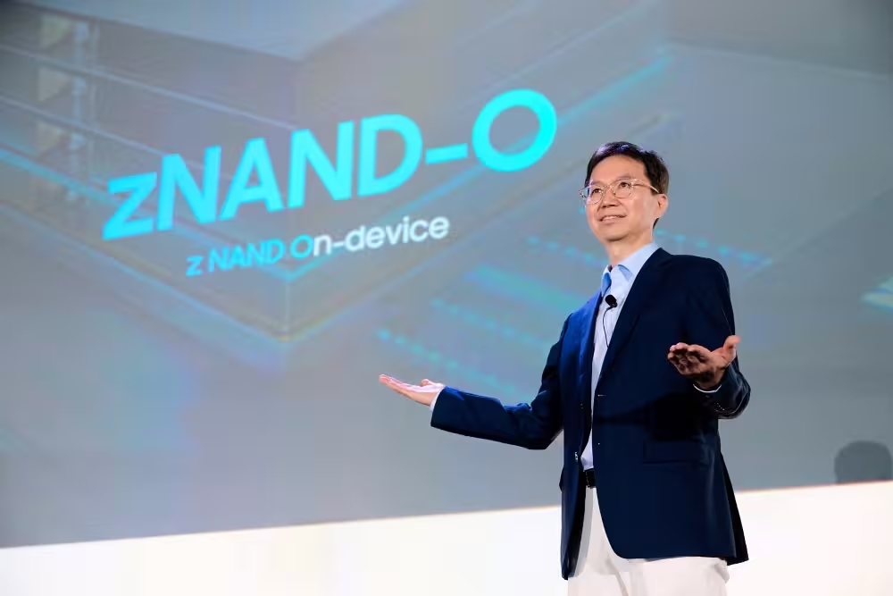
Z-NAND-O uses through-silicon via (TSV) technology to stack NAND chips vertically in four or eight layers. Samsung says Z-NAND-O aims to improve data transfer speeds and power efficiency for on-device AI on mobile and other connected devices.
Z-NAND-T focuses on throughput and bandwidth, targeting high-performance AI data centers that need to move large amounts of data efficiently.
Z-NAND-I prioritizes input/output operations per second, measuring how many individual read and write operations memory can handle.
Samsung has not officially announced the full lineup, specifications or launch timelines for the three variants.
The three-way approach suggests Samsung intends to tailor NAND technology to specific AI workloads rather than rely on a single design.
SK Hynix is pursuing a similar strategy with an AI-NAND family comprising AIN P for performance, AIN D for storage density and AIN B for bandwidth.
As AI infrastructure expands, customized NAND could become increasingly important alongside conventional memory and storage.

Leave a Comment
Comments
No comments yet. Be the first.