6 Minutes
A new direction for flat optics
Researchers working on next-generation optical components have moved beyond single-layer metasurfaces to a stacked, multilayer metalens architecture that expands what flat optics can do. Rather than continuing with incremental tweaks to conventional designs, the team adopted an inverse design workflow based on shape optimization. That change unlocked far greater design freedom and delivered practical improvements in performance and manufacturability.
From single-surface constraints to layered freedom
The decision to adopt a multi-layer metalens was born out of a design limitation: single-layer metasurfaces struggle to simultaneously control phase, amplitude and polarization across a wide range of conditions. By introducing multiple closely spaced metasurface layers, the researchers opened up a larger design space and then used an automated algorithm to explore it. The inverse design routine parameterized a wide variety of nanoscale element geometries and iteratively searched for structures that produced the desired optical response at target wavelengths.
Instead of handcrafting each element, the algorithm was guided to find metasurface geometries that produced simultaneous electric and magnetic dipole resonances at the same wavelength — a condition commonly referred to as Huygens resonances. Exploiting those resonances made it possible to achieve full 0 to 2π phase control at a single wavelength while keeping designs robust to polarization and fabrication tolerances. These properties are critical for moving from lab prototypes to scalable production for industrial and commercial optics.
Unexpected geometries from automated design
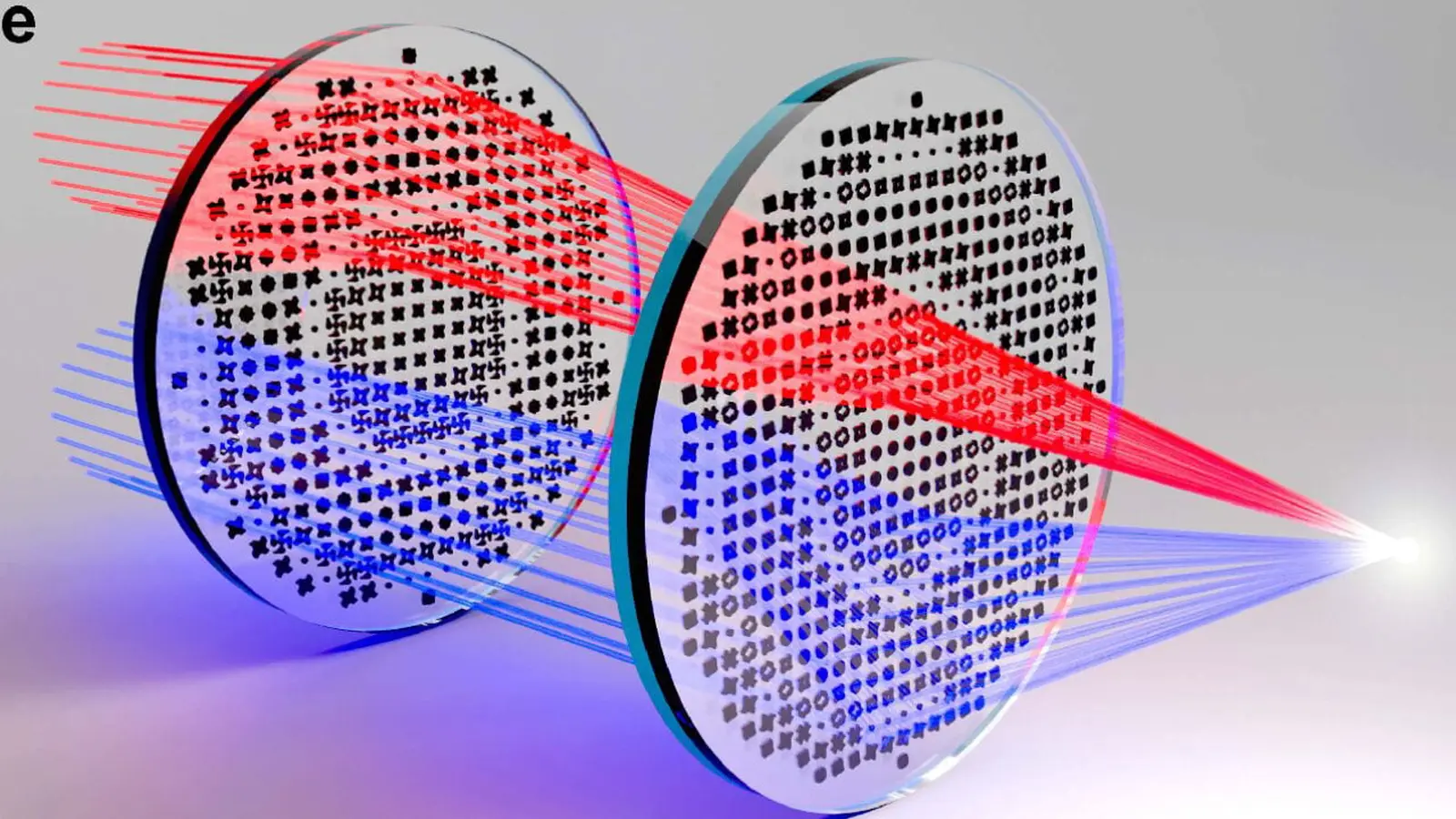
The optimization routine produced a surprisingly diverse library of metamaterial elements. Rather than simple rods or circular pillars, the algorithm returned shapes such as rounded squares, four-leaf clover motifs and tiny propeller-like structures. Each element was tuned to deliver specific phase shifts and to couple electric and magnetic responses in the intended way.
These building blocks are extremely small — on the order of a few hundred nanometres in height and roughly a thousand nanometres across — and collectively cover the full phase range needed to sculpt wavefronts. With a phase gradient map built from these elements, the team could generate arbitrary focusing patterns, not just the canonical spot produced by a conventional lens. Initially the group aimed for a simple circular focus, but the same toolkit can produce rings, off-axis focal points, or more complex focal distributions.
What the approach achieves
Key improvements enabled by the approach include:
- Polarization insensitivity: Designs using paired electric and magnetic resonances reduce the dependence on input polarization.
- Fabrication tolerance: Shape-optimized metasurfaces show greater resilience to lithographic variation, which helps with yield in manufacturing.
- Phase control: The library spans 0 to 2π phase shifts, enabling precise wavefront engineering.
These gains make multilayer metalenses more attractive for real-world imaging and sensing applications where consistency and mass-production are important.
Trade-offs and wavelength limits
The multilayer strategy is not without constraints. One practical limitation is the number of wavelengths that can be handled simultaneously. According to the research team, multilayer stacking is effective for routing or focusing a small set of discrete wavelengths — up to about five — before diffractive effects and resonance-size trade-offs begin to interfere.
That limit stems from two competing requirements. To resonate at the longest targeted wavelength, elements must be large enough; however, those large features can start to diffract shorter wavelengths in undesired ways. Balancing resonance size and diffraction suppression sets a practical ceiling on how many distinct wavelengths a single multilayer assembly can manipulate reliably.
Quote from the lab

PhD researcher Joshua Jordaan, who led much of the problem solving in the lab, described the shift in approach: 'We realized we needed a more complex structure, which then led to a multi‑layer approach.' He added that multilayer designs let the team do clever things such as directing different colours to different focal positions — essentially a compact colour router — but that the method currently works best for a handful of wavelengths rather than a full broadband spectrum.
Applications: lightweight, high-collection optics
Within the practical wavelength limitations, the multilayer metalenses offer compelling benefits for portable and mission-constrained imaging systems. Because the lenses are flat, extremely thin and composed of subwavelength structures, they can significantly reduce size, weight and power (SWaP) footprints compared with conventional refractive optics made from glass.
Potential use cases include:
- Drones and unmanned aerial vehicles: lighter, low-profile imaging modules for longer flight times and easier stabilization.
- CubeSats and earth observation platforms: compact optics that reduce launch mass while preserving light collection.
- Portable scientific instruments: miniature spectrometers or microscopes where space and weight are premium.
Jordaan noted that the team prioritized keeping designs small and lightweight with those applications in mind, making this approach particularly relevant for remote sensing and mobile imaging markets.
Market context and comparison
Flat optics and metasurfaces have been an active research area for a decade, with earlier single-layer metalenses demonstrating impressive capabilities but often facing trade-offs in polarization sensitivity, efficiency and manufacturability. The multilayer, shape-optimized approach addresses several of those weaknesses, positioning it closer to industrial adoption.
Compared to conventional multi-element glass lenses, multilayer metalenses could offer lower cost at high volume — provided fabrication processes can be standardized. Compared to single-layer metasurfaces, the stacked design gains flexibility and robustness at the cost of increased fabrication complexity.
Outlook: near-term adoption and future research
The immediate outlook is pragmatic. Multilayer metalenses are unlikely to replace high-end refractive optics across all applications in the short term, but they are well suited for niches where size, weight and specialized wavefront control matter most. Research will continue on extending bandwidth, improving efficiency across multiple wavelengths, and refining scalable manufacturing.
Areas that will likely see ongoing work include:
- Better broadband designs that mitigate diffraction trade-offs.
- Integration with detectors and sensors to create compact imaging modules.
- Process engineering to increase yield and reduce cost for volume fabrication.
Takeaway
By combining inverse design and shape optimization with a multilayer metasurface architecture, researchers have created metalens designs that are more tolerant to fabrication error and less sensitive to polarization while offering flexible wavefront control. These strengths make multilayer metalenses a promising candidate for lightweight imaging systems in drones, satellites and other portable devices — provided the limit on simultaneous wavelengths is acceptable for the target application. As design tools and nanofabrication scale up, expect to see these flat, high-performance optics migrate from research labs into practical products.
Comments
No comments yet.
Leave a Comment