3 Minutes
Huawei has quietly filed a patent that outlines a surprising route to 2 nm-class chips using only deep-ultraviolet (DUV) lithography — the very tools still available to it despite Western export controls that block extreme-ultraviolet (EUV) machines from ASML. The move, revealed in a long-hidden 2022 filing, could reshape how China’s chipset ambitions are perceived worldwide.
How Huawei aims to push DUV to the edge
The recently surfaced patent — first spotted by semiconductor researcher Dr. Frederick Chen — describes an optimized Self-Aligned Quadruple Patterning (SAQP) workflow. The technique reportedly targets an ultra-tight 21 nm metal pitch, a critical dimension that would place the resulting node in the same league as so-called "2 nm-class" processes announced by TSMC and Samsung.
Crucially, Huawei’s approach claims to cut the number of DUV exposures down to four, a dramatic reduction from traditional multi-patterning flows that require many more passes and introduce heavy complexity. If realizable, that optimization would let Huawei and manufacturing partner SMIC squeeze finer features from legacy lithography tools instead of relying on restricted EUV scanners.
Why the patent matters — and what it doesn’t prove
On paper, the idea is audacious: leapfrog from the recently demonstrated Kirin 9030 (built on SMIC’s N+3 node) to a 2 nm-generation offering without ever touching EUV. But papers and patents are one thing; high-volume production is another.
- Yield risk: Quadruple patterning at sub-3 nm dimensions is notoriously defect-prone. Each additional litho pass multiplies opportunities for overlay and particle problems.
- Cost pressure: Multiple DUV exposures raise manufacturing cost and throughput penalties. EUV’s single-exposure approach was adopted industry-wide precisely to avoid those bills.
- Tool limitations: Even highly optimized SAQP relies on extremely precise process control, etch uniformity, and metrology — areas where decades of tool integration matter.
So while the patent signals intent and engineering creativity, many industry analysts remain skeptical that a DUV-only process can match EUV-based 2 nm nodes in economic and yield terms.
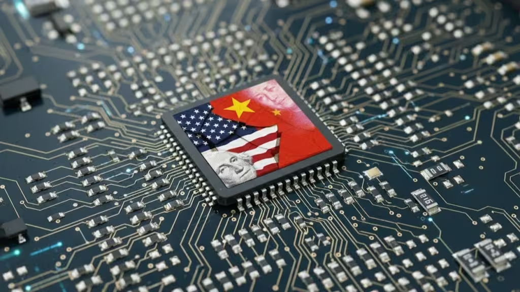
Strategic implications: technology, sanctions, and self-reliance
If Huawei and SMIC could execute a commercially viable SAQP-based 2 nm node, it would represent a major technological rebuttal to export restrictions and a boost for China’s push toward semiconductor self-sufficiency. Even absent mass production, the patent functions as a strategic statement: China will continue to innovate around sanctions, pushing legacy equipment to novel limits.
Imagine a world where cheaper, older tools are stretched to produce cutting-edge chips — it’s a provocative idea, but one that requires breakthroughs in yield engineering, process control, and supply-chain support to be more than a clever workaround.
What to watch next
Keep an eye on three indicators: any public roadmap or samples from SMIC demonstrating 21 nm metal pitch, further peer-reviewed analyses of the patent’s process flow, and signs of investment in metrology and defect reduction tools in China. Those signals will tell whether this is a patent as posture — or the first step toward a substantive manufacturing alternative to EUV.
Source: gizmochina
Leave a Comment