6 Minutes
Researchers at Tsinghua University have unveiled an integrated optical computing chip that pushes feature extraction speeds beyond the 10 GHz threshold — a milestone with implications for high-frequency trading, medical imaging, and real-time AI. By moving a key layer of computation from electricity to light, the team reports dramatically lower latency and a path to lighter, faster hybrid AI systems.
Why light? The bottleneck in modern AI computing
Modern AI and data-driven systems — from surgical robots to automated trading engines — need to sift massive, continuous data streams and extract meaningful features in milliseconds or less. Traditional electronic processors, however, are approaching physical and thermal limits. Increasing clock speeds and packing more transistors onto chips no longer scales as before: electronic interconnects and memory access impose latency and energy costs that become prohibitive for ultra-low-latency applications.
Optical computing replaces electrons with photons to perform certain mathematical operations at the speed of light. Photonics offers near-instantaneous data propagation, natural parallelism (many wavelengths and spatial channels at once), and potentially much lower energy per operation. One promising approach uses diffraction-based optical operators: thin optical elements that transform incoming light fields into desired output patterns, effectively performing linear algebra such as matrix-vector multiplications in a single pass.
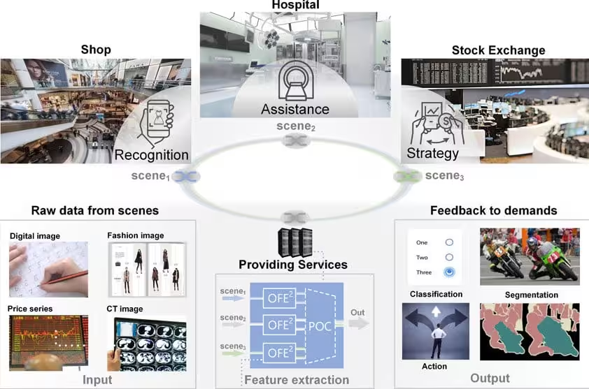
OFE2 can facilitate flexible allocation to meet multitasking demands for applications in scene recognition, medical assistance, and digital finance.
How OFE2 overcomes coherence and stability challenges
The new device, called OFE2 (optical feature extraction engine 2), addresses a core limitation of coherent optical computing: maintaining stable phase relationships among parallel optical channels at very high speeds. Many photonic systems use fiber-based splitters and delay lines to create multiple data channels, but fibers introduce phase noise and temperature-sensitive perturbations that limit operating frequency.
To solve this, the Tsinghua team developed an integrated on-chip data-preparation module featuring tunable power splitters and precisely controlled delay lines. This module samples an incoming serial data stream and deserializes it into multiple stable parallel optical branches. An adjustable integrated phase array then lets the device reconfigure how those branches interfere at the diffraction operator, enabling the chip to steer optical energy to chosen outputs and realize specific feature detectors.
Diffraction as computation: matrix operations in a beam
When properly configured, the diffraction operator behaves like a programmed matrix. Incoming waves—each carrying a piece of the data—interfere as they travel through the diffractive element, and the resulting pattern produces a focused bright spot whose position and intensity encode the result of a matrix-vector multiplication. By tracking how output power shifts with time or input variations, OFE2 extracts features such as image edges or temporal patterns in market data.
Performance: 12.5 GHz and sub-250 ps latency
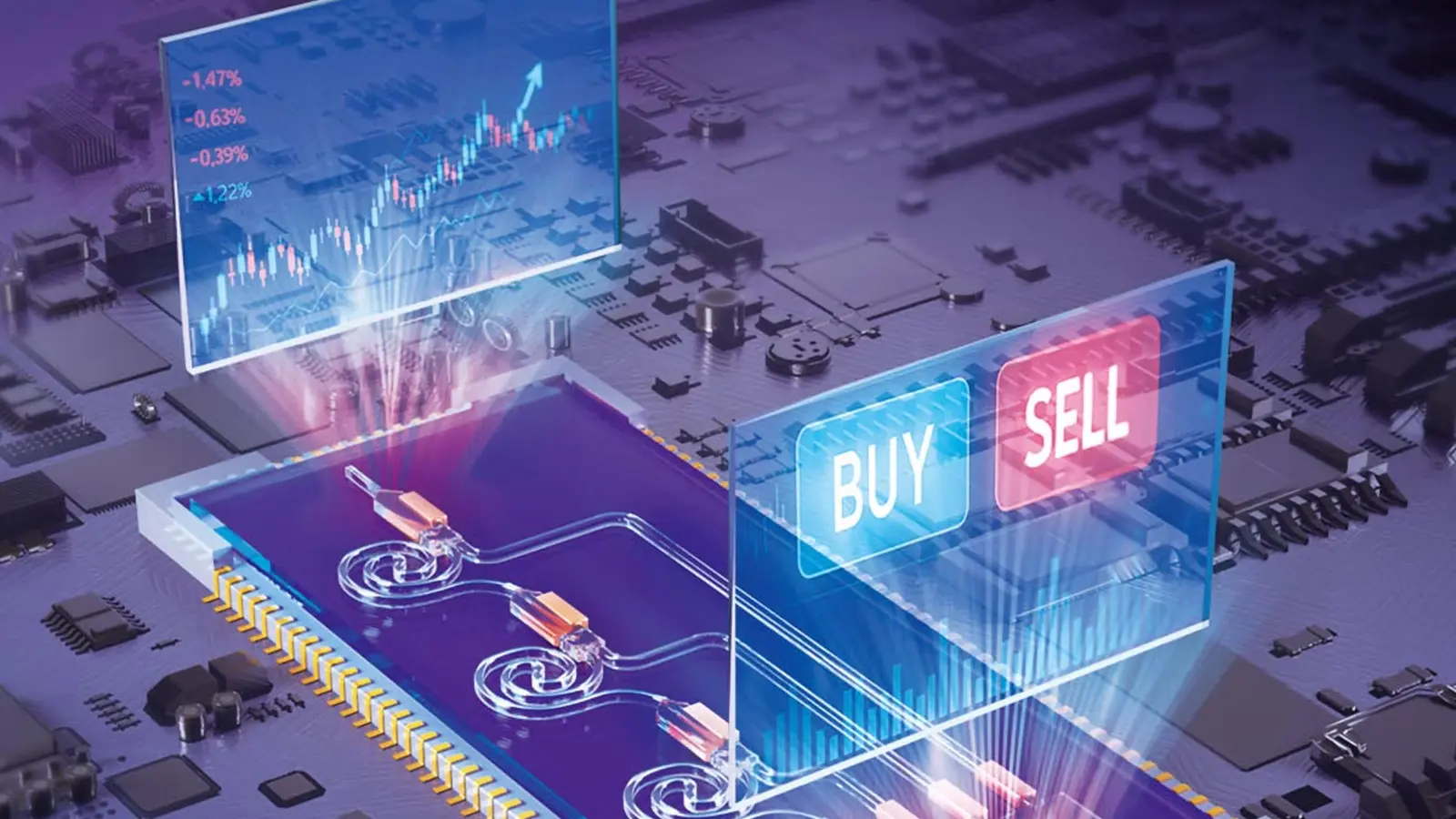
OFE2 operates at an effective rate of 12.5 GHz. The team reports that a single matrix-vector multiplication completes in under 250.5 picoseconds, making this implementation one of the fastest integrated optical computing demonstrations to date. That sub-nanosecond latency matters when every microsecond counts — for example, in algorithmic trading strategies where small delays can swing profitability.
Crucially, the optical pre-processing stage reduced the burden on downstream electronic neural networks. In image tasks, OFE2 generated complementary 'relief and engraving' feature maps that improved classification accuracy and boosted pixel-wise performance in semantic segmentation (such as organ identification in CT scans) while requiring fewer electronic parameters than a baseline purely electronic pipeline.
Real-world tests: images and market signals
The researchers validated OFE2 on both visual and financial workloads. In imaging experiments the diffractive engine reliably highlighted edges and texture features that made subsequent neural-network classification and segmentation more accurate and efficient. For a digital trading task, time-series price signals fed into OFE2 were mapped to trading actions after training; the optical outputs could be converted directly to buy/sell decisions via a simple thresholding step, enabling a trading loop executed at photonic speeds.
Because the core computations happen in passive optical components, energy consumption per operation can be dramatically lower than conventional electronic pre-processing. That offers a practical route to hybrid architectures where photonics handles the most intense, latency-sensitive front-end tasks and electronics perform higher-level decision making.
Related technologies and next steps
OFE2 sits within a growing ecosystem of integrated photonics research: programmable photonic circuits, neuromorphic photonic processors, and wavelength-division multiplexed optical accelerators. Key challenges remain — integrating reliable optical sources, packaging for thermal stability, manufacturing repeatability, and developing design tools that map machine-learning models to physical diffractive layouts.
The Tsinghua team published their results in Advanced Photonics Nexus and signaled interest in partnering with groups that have data-intensive, latency-critical workloads. Moving from lab prototypes to deployment will require co-design with application vendors — financial firms, medical-device manufacturers, and imaging companies — to ensure interfaces, control electronics, and algorithms are production-ready.
Expert Insight
Dr. Maria Alvarez, a photonics systems engineer (fictional), comments: 'This work demonstrates a practical path for pushing optical computing into applications that demand both speed and configurability. Integrated data-preparation on chip is the kind of engineering advance that bridges proof-of-concept optics and useful, deployable accelerators. We're still a way from replacing GPUs entirely, but hybrid photonic-electronic stacks could change how we architect low-latency AI systems.'
Looking ahead, combining OFE2-style diffraction operators with compact lasers and on-chip detectors could produce ultra-fast sensors and edge processors for robotics, autonomous vehicles, and finance. As photonic fabrication matures and algorithms adapt to optical constraints, expect more hybrid systems that exploit light where it matters most: at the front lines of data arrival.
Source: scitechdaily
Comments
labcore
seen similar diffractive prototypes in the lab, losses and detector mismatch are nasty, you need co designed lasers and sensors. still curious to see live demos
mechbyte
If they really nailed 12.5 GHz on chip and stability, wow... but can it survive real world packaging and temp shifts? sounds huge, yet i'm wary
Leave a Comment