
3 Minutes
Researchers from New York University and the University of Queensland have demonstrated superconductivity in gallium-doped epitaxial germanium — a development that could reshape how quantum chips are built at wafer scale.
A wafer-scale surprise: superconducting germanium
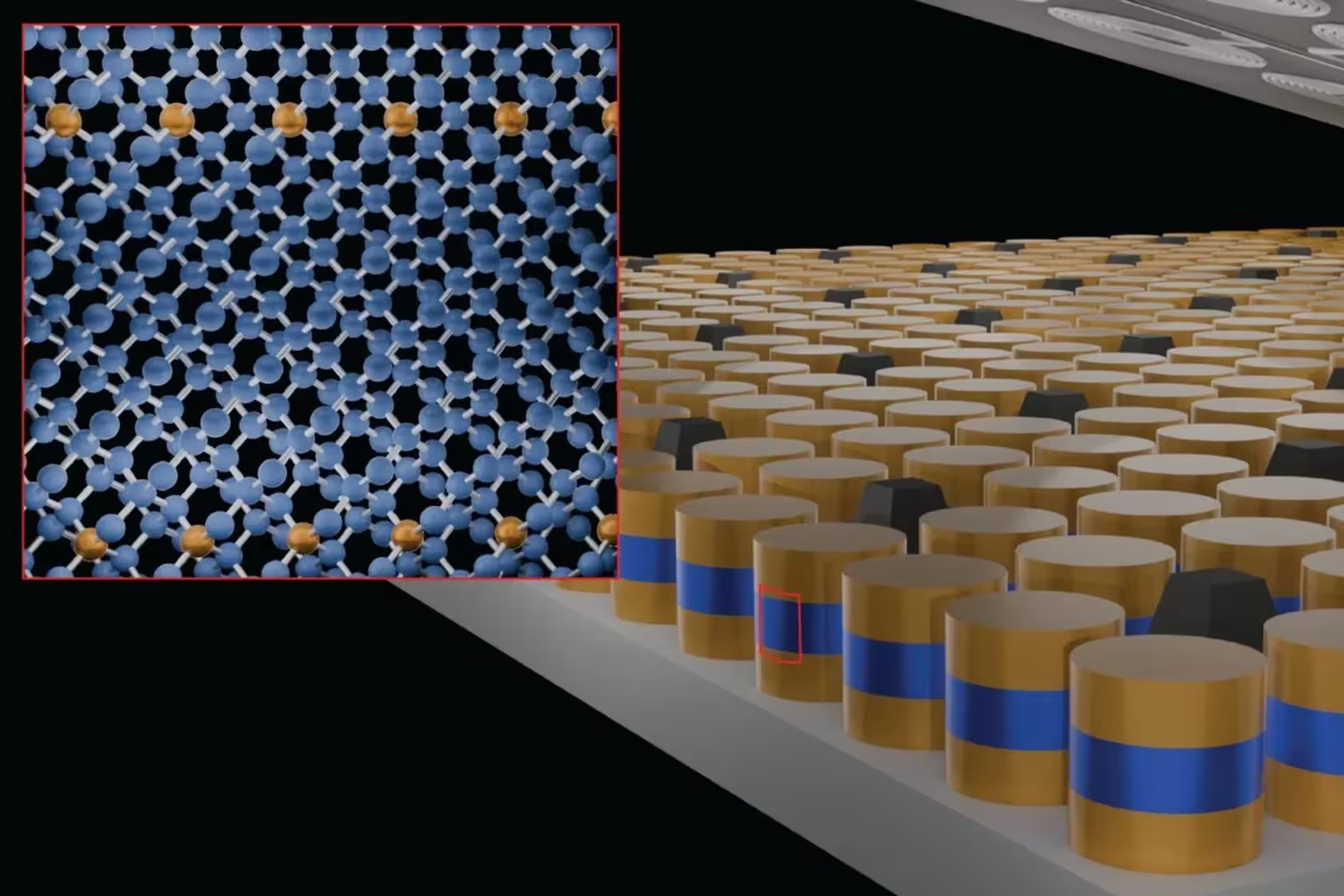
In a milestone paper published in Nature, the team showed that germanium grown by standard semiconductor methods becomes superconducting when doped with gallium. The superconducting transition occurs below about 3.5 kelvin, and — crucially — the material supports dense arrays of Josephson junctions across a full two-inch wafer. Imagine millions of superconducting contacts patterned with industry-grade lithography and tested at cryogenic temperatures to confirm robust superconducting behavior and practical current densities.
How they made it: clean layers, precise doping
The group used molecular beam epitaxy (MBE) to grow ultra-clean germanium films and place gallium atoms into precise lattice sites. By raising the dopant concentration past a critical threshold, the germanium film flips into a superconducting phase while keeping interfaces defect-free. That clean, layer-by-layer growth prevents the rough boundaries that often kill device performance.
Why this matters: compatibility and scaling
What sets this work apart is manufacturability. The gallium-doped germanium was created with processes similar to those already used in compound-semiconductor and Cryo-CMOS production, making it compatible with existing fabs. That could remove long-standing barriers to integrating semiconductor logic with superconducting elements — lowering parasitic capacitance, reducing thermal losses, and enabling far denser quantum circuits than today’s approaches allow.
In practice, the result is a path from isolated lab-scale flakes to wafer-scale superconducting circuitry suitable for quantum processors, cryogenic RF systems, low-noise sensors, and even space-qualified electronics.
Challenges ahead and the roadmap to integration
Next, the researchers will tackle scaling to larger wafers, improving process repeatability, and demonstrating reliable integration of superconducting germanium with silicon-based logic. If those steps succeed, superconducting germanium could become a practical platform for industrial-scale quantum chips — combining the best of semiconductor fabrication with superconducting circuit performance.
Could germanium be the key to mass-producible quantum hardware? The early results are promising, and this wafer-scale approach makes that question one the semiconductor industry will be watching closely.
Leave a Comment