6 Minutes
Researchers have turned a mainstream semiconductor — germanium — into a superconductor for the first time, opening a new path toward energy-efficient quantum chips and cryogenic electronics. By embedding gallium atoms into germanium’s crystal lattice with atomic precision, the team created a stable, zero-resistance material that can be manufactured at wafer scale.
Why turning germanium superconducting matters
Semiconductors like silicon and germanium are the backbone of modern electronics, but they normally resist the flow of electrons and generate heat. Superconductors, in contrast, carry current with zero resistance. Combining both behaviors in the same material could collapse the interface losses that plague hybrid devices, dramatically improving performance for classical computing, cryogenic control electronics and quantum processors.
"Establishing superconductivity in germanium, which is already widely used in computer chips and fiber optics, can potentially revolutionize scores of consumer products and industrial technologies," says Javad Shabani, director of NYU's Center for Quantum Information Physics and Quantum Institute, who led the research. Peter Jacobson of the University of Queensland adds that the work "could accelerate progress in building practical quantum systems" by enabling clean, scalable boundaries between superconducting and semiconducting regions.
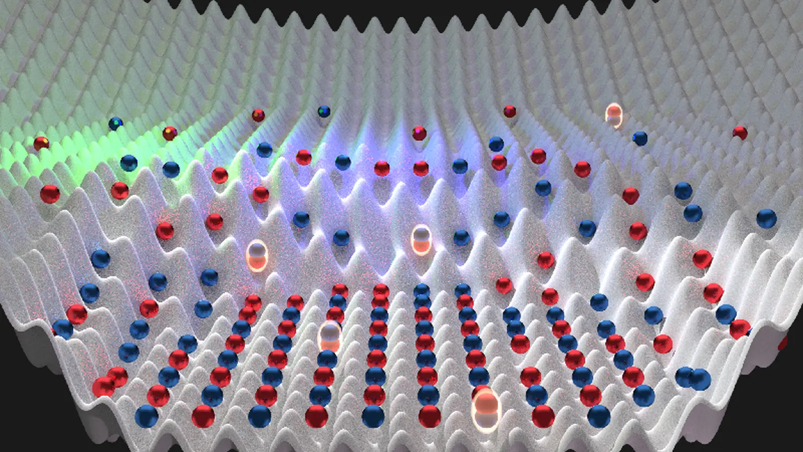
.avif)
Josephson junction structures—quantum devices made of two superconductors and a thin non-superconducting barrier—using different forms of germanium (Ge): super-Ge (in gold), semiconducting Ge (in blue), and super-Ge on wafer-level scale. Millions of Josephson junction pixels (10 micrometer square) can be created with this new material stack on wafer scale. Inset shows crystalline form of Super-Ge on the same matrix of semiconductor Ge, a key for crystalline Josephson junction.
Historically, turning group-IV semiconductors (like silicon and germanium) into superconductors is challenging. High dopant concentrations tend to destabilize the crystal lattice, and imprecise methods disrupt the atomic order required for electron pairing — the microscopic mechanism for superconductivity. The new study overcomes these barriers by combining high-precision growth with detailed structural diagnostics.
How the team engineered superconducting germanium
The core advance is materials-level control. Rather than implanting ions — a rough, often-damaging technique — the researchers used molecular beam epitaxy (MBE) to grow thin germanium films while incorporating gallium atoms into the lattice. Gallium acts as a dopant that increases mobile charge carriers, but at high concentrations it normally breaks the crystal. Using MBE lets atoms arrange themselves gently during growth, preserving crystalline order even when many gallium atoms substitute for germanium.
Advanced X-ray measurements guided the optimization. Those structural probes revealed how gallium occupies lattice sites and how much distortion the crystal tolerates before superconductivity is suppressed. By tuning the growth conditions, the team produced a crystalline “super-Ge” phase that supports zero-resistance current flow below about 3.5 Kelvin (roughly -453 °F).
Julian Steele, a co-author from the University of Queensland, explains: "Using epitaxy — growing thin crystal layers — means we can finally achieve the structural precision needed to understand and control how superconductivity emerges in these materials." The study also included collaborators from ETH Zurich and Ohio State University and received partial support from the U.S. Air Force Office of Scientific Research.
From lab demonstration to wafer-scale quantum devices
One of the most striking claims in the research is manufacturability. The super-Ge material stack can be grown at wafer scale, enabling the fabrication of millions of Josephson-junction pixels (10 µm squares) on a single wafer. Josephson junctions are the fundamental building blocks of many superconducting quantum circuits and sensors. Creating them directly from crystalline germanium layers removes complex hybrid interfaces and could simplify integration with existing semiconductor foundries.
Potential applications include:
- Foundry-compatible quantum bits (qubits) and superconducting interconnects that sit naturally on the same wafer as semiconducting control electronics.
- Low-power cryogenic control chips for large-scale quantum processors, reducing heat load and wiring complexity at millikelvin temperatures.
- High-sensitivity sensors and superconducting microwave circuits with improved coherence due to cleaner atomic interfaces.
Because germanium is already a workhorse for advanced semiconductor processes and fiber-optic components, converting it to a superconductor without wholesale changes to fabrication could accelerate commercialization. The ability to tune superconductivity via controlled gallium substitution also provides a new platform to study the physics of electron pairing in group-IV materials.
Expert Insight
Dr. Elisa Moreno, a fictional materials scientist specializing in quantum device integration, comments: "This result is a practical game-changer. Achieving superconductivity in a material that is already in foundries removes a major barrier between experimental quantum hardware and scalable manufacturing. The key will be reproducibility across wafer sizes and compatibility with backend processing — but the pathway is now clear."
Her comment underscores the pragmatic focus of the discovery: it is not just a physics milestone, but a materials-engineering solution that bridges the gap between laboratory superconductors and industrial semiconductor workflows.
Looking ahead, researchers will probe how robust the super-Ge phase is to further processing steps, whether critical temperatures can be pushed higher through alternative dopants or strain engineering, and how devices built from super-Ge perform in real-world quantum circuits. If those questions resolve favorably, the fusion of superconductivity and mainstream semiconductor technology could reshape how we design energy-efficient quantum hardware and cryogenic control systems.
Source: sciencedaily
Comments
DaNix
Is this even true? gallium at those concentrations without wrecking the lattice feels optimistic. Reproducible across full wafers? skeptical but curious
labcore
Whoa, turning germanium superconducting? mind blown. If wafer-scale Josephson pixels are real this could totally change chip manufacturing, but 3.5 K is still awfully cold…
Leave a Comment