6 Minutes
Researchers have found a clever optical trick to visualize single-atom-thick sheets of hexagonal boron nitride (hBN) — a material so transparent in the visible range that conventional microscopes struggle to see it. Using a nonlinear imaging method that converts infrared-driven lattice vibrations into visible light, scientists can now image, orient, and map hBN monolayers quickly and with high contrast.
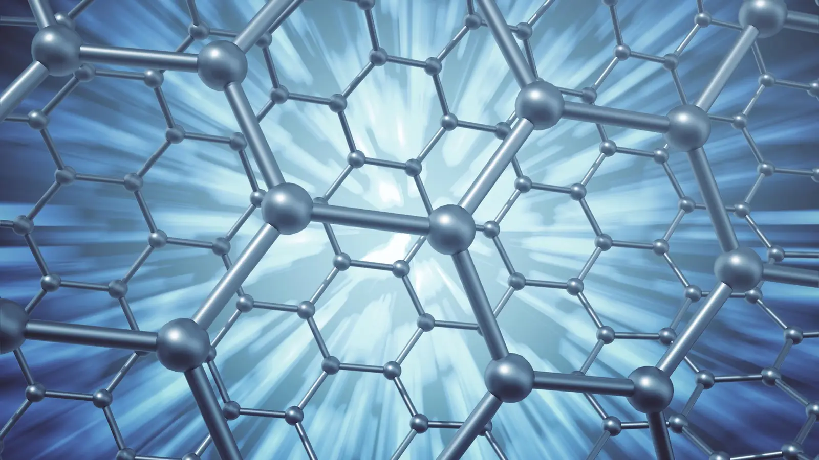
Boron nitride is a crystalline material made of boron and nitrogen atoms arranged in a hexagonal lattice, giving it a two-dimensional structure that closely resembles graphene but with distinct electronic and optical properties.
How the new microscope makes the invisible visible
At the Fritz Haber Institute (FHI) researchers combined mid-infrared and visible laser beams in a phase-resolved sum-frequency generation (SFG) microscope to coax hBN monolayers into emitting a bright optical signal. The technique takes advantage of a resonant vibrational mode in hBN: when the mid-IR light matches that vibration, the interaction with a second visible beam produces a sum-frequency output that is orders of magnitude stronger than background signals.
In plain terms: the mid-IR beam excites a lattice vibration in the one-atom-thick sheet, and the visible beam reads out that motion by generating light at the sum of the two frequencies. Because this process is resonant and nonlinear, monolayer hBN — which is essentially transparent in conventional imaging wavelengths — lights up with high contrast in the SFG detector.

SFG microscopy image of boron nitride monolayer flakes. Credit: FHI
The instrument is fast and practical. The team reports imaging areas of roughly 100 × 100 μm2 in under a second, and importantly, the phase-resolved measurement encodes crystallographic orientation as well as presence and contrast. That means grain boundaries, edge terminations and local distortions — critical details for building reliable 2D heterostructures — can be visualized in situ.
Why hexagonal boron nitride matters for 2D materials and devices
Hexagonal boron nitride, often dubbed “white graphene,” is a layered material made from alternating boron and nitrogen atoms. Like graphene, its monolayers have a hexagonal lattice, but hBN brings a complementary set of properties: a wide electronic band gap, strong mid-infrared resonances, chemical stability, and an atomically flat surface that makes it an ideal substrate or encapsulant for other 2D materials.
Because hBN is optically silent across the near-IR and visible regions when present as a single layer, routine optical inspection and alignment during fabrication has been difficult. That opacity gap limited the live assembly and quality control of stacked van der Waals heterostructures — artificial crystals made by stacking different 2D layers. The SFG approach directly addresses those limitations by offering label-free, non-invasive contrast and orientation data during fabrication workflows.

Schematic of the newly developed SFG microscope used to image the layers of boron nitride.
Beyond imaging, the detected large nonlinear optical response near the vibrational resonance suggests monolayer hBN could be used for frequency upconversion — converting infrared signals into visible light — which has potential applications in infrared photonics and optoelectronic devices. In short, the microscope is not just a metrology tool but a window into functional properties that can be harnessed in new device concepts.
Collaborative effort and technical validation
The work reflects a cross-departmental and international collaboration. hBN monolayer flakes were synthesized at Vanderbilt University, imaged via SFG microscopy at FHI’s Physical Chemistry Department, and further characterized with atomic force microscopy (AFM) by partners at Freie Universität Berlin. The FHI Theory Department then analyzed the crystallographic data to extract edge terminations and lattice orientations.
Using complementary AFM confirmed the presence and thickness of monolayers, while the SFG images delivered superior optical contrast and orientation maps in real time. The combined dataset revealed that triangular hBN domains tend to display nitrogen-terminated zigzag edges — a structural detail that can influence electronic and optical behavior when these layers are integrated into heterostructures.
Prospects for imaging broader classes of 2D materials
Because the SFG technique relies on resonantly driving vibrational modes, it could be extended to other atomically thin materials that possess distinctive infrared-active phonons or molecular vibrations. The authors anticipate the method will become a versatile, non-invasive, label-free imaging tool for fast quality control during fabrication and live assembly of multi-layer devices.
Practically speaking, that could accelerate the manufacturing of van der Waals heterostructures for quantum optics, infrared nanophotonics, and next-generation (opto-)electronic components. The ability to visualize crystal orientation in real time also opens new possibilities for twist-angle engineering — deliberately rotating layers relative to one another to create exotic electronic phases.
Expert Insight
"Seeing monolayer hBN with optical contrast is a real game-changer for 2D materials research," says Dr. Elena Márquez, a fictional materials scientist specializing in optoelectronics. "This method gives experimentalists a live, non-invasive way to align layers and detect defects that previously required slow, contact-based techniques. For laboratories building complex heterostructures, that saves time and improves reproducibility."
Dr. Márquez adds: "The frequency upconversion angle is exciting too — converting IR to visible light on a chip could be useful for sensing and communication technologies where IR detection is currently challenging or costly."
What this means for future devices and research
The newly demonstrated phase-resolved sum-frequency microscope offers a practical path to integrate hBN and other transparent 2D layers into production workflows. Faster, higher-contrast imaging combined with orientation mapping can improve defect control and enable precise stacking — essential steps toward scalable devices based on van der Waals engineering.
As the method scales and is adapted to different materials, we can expect more robust fabrication of quantum devices, infrared photonic components, and layered materials with engineered electronic behavior. For the broader community studying 2D materials, this is a valuable new tool that blends spectroscopy, microscopy, and materials science into a single, actionable technique.
Source: scitechdaily
Comments
Tomas
Looks cool, but is this robust on large wafers? if vibration peaks shift with strain, will contrast drop? curious.
atomwave
wow didn't expect that... hBN lighting up like this? fast imaging + orientation mapping = game changer, but curious about noise and real-world throughput
Leave a Comment