9 Minutes
Light-driven computing tackles AI’s energy crisis
Artificial intelligence is fueling a rapid expansion of compute demand across science, industry and everyday applications — from satellite image analysis to voice assistants and autonomous systems. But this growth comes with a rising energy bill: large neural networks and convolutional layers in particular require massive numbers of multiply-accumulate operations that translate into heavy power use in data centers and edge devices. Researchers at the University of Florida report a potentially disruptive approach: a silicon photonic chip that performs convolution operations using laser light and etched micro-lenses, offering orders-of-magnitude reductions in energy for key AI inference tasks.
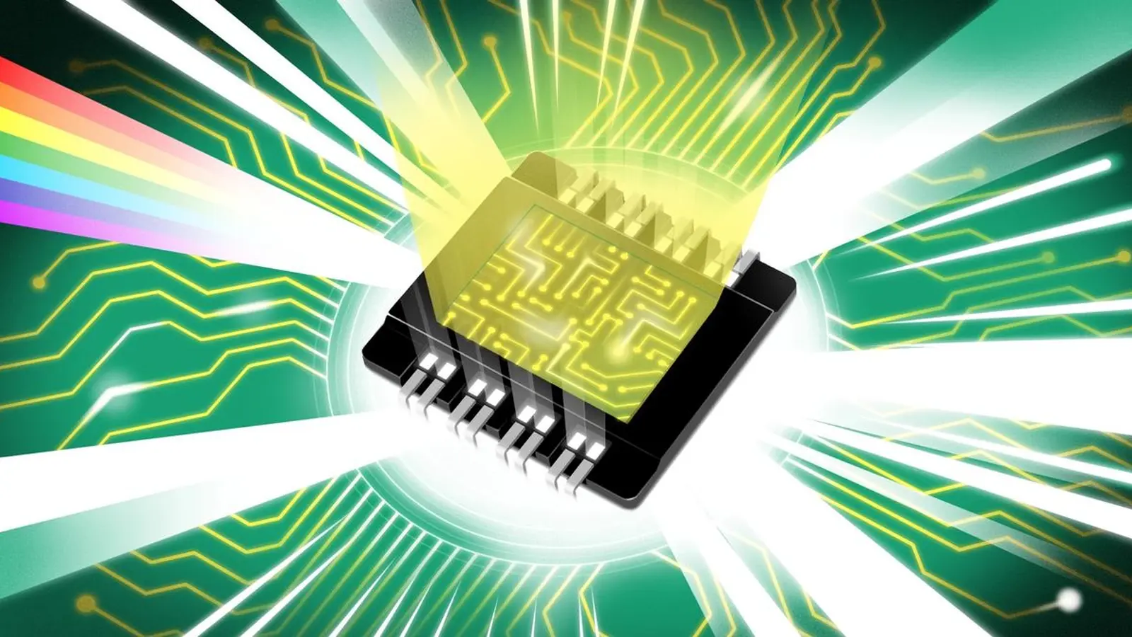
A newly developed silicon photonic chip turns light-encoded data into instant convolution results. Credit: H. Yang (University of Florida)
Published in Advanced Photonics and announced through SPIE on September 9, 2025, the work demonstrates a prototype that carries out convolutional computations on-chip by converting electrical signals into optical patterns, manipulating the light with microscopic Fresnel lenses, then converting the resulting interference patterns back into digital outputs. The team reports near-equivalent accuracy to conventional electronic implementations while reducing the energy used for the core operation by up to two orders of magnitude — a capability that could meaningfully lower the power footprint of AI inference in both data centers and power-constrained platforms such as satellites and robots.
Scientific background: why convolution matters for AI
Convolutional operations are fundamental to many machine-learning models, especially convolutional neural networks (CNNs) used for visual pattern recognition, object detection and other perceptual tasks. A convolution applies a small filter (kernel) across an array of input values (for example, pixels) and computes weighted sums that reveal local features such as edges and textures. Executing many convolutions across many layers creates the feature maps that let neural networks learn hierarchical representations. But each convolution is computationally expensive when implemented electronically, because it requires many multiply-accumulate operations executed sequentially or in large parallel arrays of transistors.
Optical computing offers an alternative: light naturally interferes and diffracts, performing linear transformations in free space or guided structures with minimal energy dissipation. In particular, optical lenses and diffractive elements can implement linear transforms (including convolutions) by shaping phase and amplitude. Leveraging these physical properties on a silicon platform — the mainstay of the semiconductor industry — opens a path to high-throughput, low-power AI hardware that integrates with existing fabrication flows.
How the photonic convolution chip works
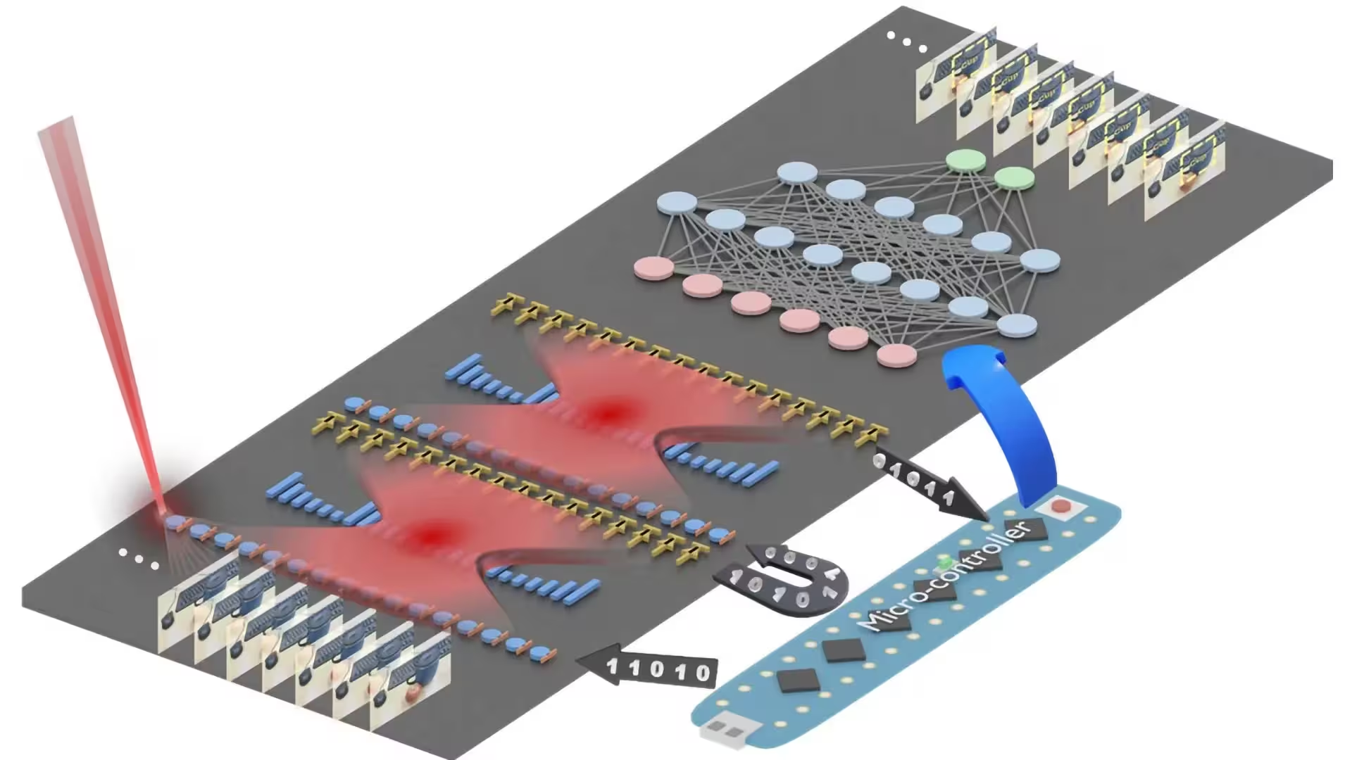
The University of Florida prototype integrates optical components directly onto a silicon substrate using semiconductor manufacturing techniques. Key elements and steps in a single inference pass include:
Data encoding and optical projection
- Input data (for example, a small image patch or a vector of pixel intensities) is encoded into light fields by modulating laser sources or using on-chip modulators.
- Multiple laser beams can be used simultaneously, each at a different wavelength, enabling parallel processing of multiple data streams through wavelength-division multiplexing.
On-chip Fresnel lenses as computational elements
- The chip uses two sets of microscopic Fresnel lenses: ultrathin, diffractive lens structures that focus and shape light equivalent to much larger curved optics.
- These lenses are patterned directly into the silicon and are narrower than a human hair. Their diffractive behavior carries out the convolution-like linear transform as the encoded light propagates through the optical train.
Detection and digitization
- After the light passes through the lens structures and interferes to produce the desired transformed wavefront, photodetectors on the chip convert the optical intensity patterns back into electrical signals.
- The electrical outputs are then post-processed by conventional electronics to finish the inference operation (activation functions, pooling, classification layers, etc.).
This sequence performs the multiply-accumulate heavy-lifting in the optical domain, where propagation and diffraction impose negligible energy cost compared to electronic multiplication.
Experimental results, accuracy and scalability
In laboratory tests the prototype performed image-classification tasks such as identifying handwritten digits with roughly 98% accuracy — comparable to purely electronic baseline implementations for the same network architecture and dataset. Crucially, the authors report that the optical convolution stage operates at near-zero incremental energy relative to equivalent electronic multiply-accumulate units, enabling overall energy reductions on the order of 100× for the convolution-heavy portions of inference.
The team also demonstrated wavelength multiplexing: by injecting different colors of laser light through the same lens structures, the chip processed multiple kernels simultaneously without adding proportional energy cost or chip area. This spectral parallelism is intrinsic to photonics and provides a route to further scale throughput without classic transistor scaling.
However, the prototype is an early-stage device. Challenges remain in integrating photonic convolutional layers into full-scale neural network accelerators, including: high-fidelity on-chip modulators and detectors, managing noise and crosstalk, aligning optical and electronic interfaces, and handling programmability and reconfigurability for different kernels and network topologies. The conversion steps (electrical-to-optical and optical-to-electrical) also introduce latency and nonzero energy overhead that must be optimized for overall system gains.
Implications and potential applications
If matured and mass-produced, silicon photonic convolution modules could reshape where and how AI inference is performed. Potential impacts include:
- Data center energy reduction: Offloading convolution-heavy layers to optical hardware could significantly cut operational power in cloud inference farms.
- Edge and space-borne AI: Lightweight, low-energy photonic accelerators are attractive for satellites, planetary probes and remote sensing platforms where power and thermal budgets are constrained.
- Real-time embedded systems: Robotics, autonomous vehicles and drones could benefit from higher throughput and lower power for vision and lidar processing.
The researchers emphasize compatibility with standard semiconductor fabrication, which may ease adoption by existing chip manufacturers and foundries. They also note that companies already using optical interconnects or optical co-processors in specialized AI stacks could integrate photonic convolution units into hybrid optoelectronic accelerators.
Expert Insight
Dr. Samuel Kim, senior photonics engineer with 15 years of experience in space instrumentation, offers perspective: "This work advances the practical integration of diffractive optics directly on silicon, which is a crucial step. For space and remote systems, reducing the energy per inference by two orders of magnitude is transformative — it could allow more sophisticated onboard analysis without adding solar panels or radiators. The main challenges I see are ensuring robustness to radiation and temperature variations, and delivering programmable reconfigurability so the hardware can support a range of models in the field."
Dr. Kim adds that wavelength multiplexing is particularly promising: "Multiplexing leverages a dimension that electronics can't exploit easily. If packaging and multi-wavelength light sources are made compact and reliable, throughput could scale in a way that supplements Moore's Law for AI workloads."
Related technologies and future prospects
The photonic-convolution approach fits into a broader ecosystem of optical and hybrid computing research. Related lines of work include: integrated Mach–Zehnder interferometer meshes for matrix-vector multiplication, diffractive deep neural networks fabricated as free-space optics, and on-chip photonic memory concepts. Each approach balances different trade-offs in programmability, precision, footprint and energy efficiency.
Progress in semiconductor photonics — stronger modulators, lower-loss waveguides, compact multi-wavelength laser sources and integrated photodetectors — will determine how rapidly optical computing components move from prototypes to commercial accelerators. Collaboration between academia, national labs and industry (including vendors already deploying optical elements in AI systems) will be important to bridge the engineering gaps and establish manufacturing pipelines.
Limitations and open questions
Several technical and system-level uncertainties remain:
- Precision and noise: Optical intensity encoding is susceptible to detector noise and limited dynamic range, which can affect numerical precision for deep networks or training tasks.
- Programmability: Convolution kernels in many networks are learned during training and may need frequent updates. Optical elements must support reconfigurability or be paired with programmable electronic layers.
- System integration: Hybrid optical-electronic systems require efficient interfaces and co-design of software stacks to route workloads optimally.
- Lifecycle and reliability: For deployment in harsh environments (space, industrial), photonic devices must meet stringent reliability standards.
Addressing these topics will be a focus of follow-on research and industrial development.
Conclusion
The University of Florida’s silicon photonic convolution chip demonstrates a compelling pathway to drastically reduce the energy cost of a core AI operation by harnessing light. By etching microscopic Fresnel lenses on silicon and encoding data into laser beams, the prototype performs convolutional transforms with competitive accuracy and orders-of-magnitude lower energy for the optical stage. Wavelength multiplexing and compatibility with semiconductor fabrication strengthen the case for broader adoption.
While practical deployment requires solving challenges in programmability, integration and reliability, the work highlights a viable optical strategy to expand AI capability without proportionally expanding energy consumption. For energy-constrained systems — from edge devices to satellites to large-scale data centers — chip-based photonics could become an essential tool in the next wave of AI hardware innovation.
Source: sciencedaily
Leave a Comment