
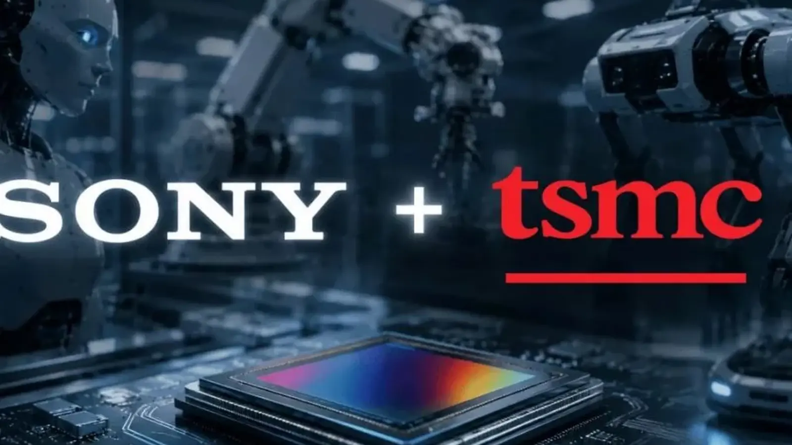
Imagine a camera sensor so capable it changes how machines see. That’s what two industry giants are quietly betting on.
Sony and Taiwan Semiconductor Manufacturing Company (TSMC) plan to pour roughly 1 trillion yen—about $6.3 billion—into a joint venture to develop and fabricate next-generation image sensors. The venture will be structured with Sony holding approximately 60 percent and TSMC about 40 percent of the new company, and commercial production is slated to begin in 2029 in Kumamoto, on Japan’s southern island.
The move is more than an equipment upgrade. It’s a strategic recalibration. Sony brings decades of leadership in sensor design and optical know-how. TSMC brings the world’s most advanced contract foundry capabilities and chip processing expertise. Together they aim to shrink pixel sizes, boost sensitivity, and accelerate on-chip processing—features that matter when cameras stop being just cameras and start acting like brains for machines.
This partnership is designed to fuse Sony’s imaging mastery with TSMC’s manufacturing scale and process innovation.
Why now? The answer is obvious once you lift the hood: the next wave of growth in imaging won’t come from selfies. It will come from AI-driven systems that need richer, faster visual data—automotive safety stacks, industrial robots, and a new generation of smart devices. Both companies have signaled they’ll explore those physical-AI applications as part of the collaboration, sizing the market beyond phones and into vehicles and factories.
For Sony, already the world’s largest image-sensor maker, this doubles down on a core business at a moment when sensor performance can set winners apart across multiple industries. For TSMC, the partnership extends its foundry reach into highly specialized imaging processes that require tight integration between design and manufacturing.
Building a cutting-edge fab in Kumamoto also has geopolitical and supply-chain logic. Locating production in Japan brings proximity to key customers, leverages local talent, and diversifies global capacity amid rising demand for sophisticated vision chips.
There are technical challenges ahead—advanced lithography, thermal management, and integrating AI preprocessing on tiny silicon die are not trivial problems. But when two leaders combine complementary strengths, the odds of meaningful innovation rise.
Expect competitors and customers to watch closely. If the joint venture delivers on performance and yields, the ripple effects could reshape how companies think about vision sensors and where they get them.
Who benefits? End users get smarter devices. Automakers and robotics firms get better perception stacks. And the semiconductor supply chain gets another large-scale project that tightens the link between design brilliance and manufacturing muscle.
It’s a big bet. And in a world driven increasingly by sight, it might just be the one that changes everything.

Leave a Comment
Comments
No comments yet. Be the first.