3 Minutes
TSMC has kicked off construction on what it calls its most advanced chip plant yet — a $48.5 billion Angstrom-era facility in Taichung that will manufacture the company’s A14 (1.4nm) process. The move signals an aggressive push into next-generation nodes while balancing global capacity for customers from mobile to high-performance computing.
A $48.5 billion bet on the Angstrom era
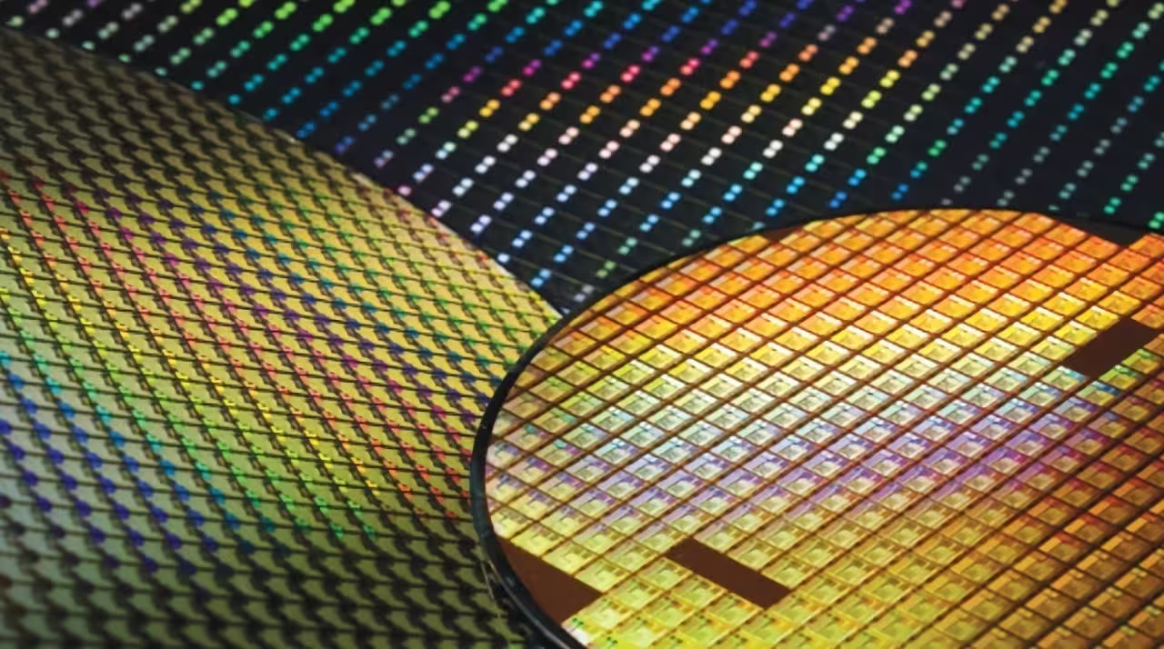
The Taiwan Economic Daily reports TSMC has started building the 1.4nm campus in central Taiwan. The multi-fab complex will include four fabs, with the first slated to come online by the end of 2027 and initial mass production expected around 2028. Early output is estimated at roughly 50,000 wafers when that first fab ramps.
Why TSMC pivoted from 2nm to 1.4nm
Originally planned as a 2nm site, TSMC upgraded the Taichung project to an Angstrom-level node as part of a broader capacity strategy. The company intends to place a sizable portion of 2nm output in its U.S. facilities to meet strong demand from high-performance computing (HPC) and mobile clients. By keeping its bleeding-edge A14 production in Taiwan, TSMC aims to concentrate the most advanced processes at home while expanding older-node capacity overseas.
How the A14 (1.4nm) will be manufactured
One striking technical choice: the A14 node won’t rely on High-NA EUV lithography. Instead, TSMC plans to use advanced multi-patterning techniques to reach Angstrom-class densities. That contrasts with competitors like Intel, which intends to use High-NA EUV for its 14A node. The decision highlights differing engineering trade-offs — cost, yield, and supply chain readiness — as foundries race to extend Moore’s Law.
Who will buy chips from the A14 node?
Customers expected to drive demand include major mobile SoC designers such as Apple, Qualcomm, and MediaTek. At the same time, HPC firms like NVIDIA and AMD are likely to tap A14 for next-generation AI accelerators and data-center processors. In short, the node is being positioned to serve both mobile devices and heavy-duty AI workloads.
- Location: Taichung, central Taiwan
- Project cost: approximately $48.5 billion
- Node name: A14 (1.4nm, Angstrom era)
- Fabs: four on the campus; first online end of 2027
- Initial throughput: ~50,000 wafers at first ramp
- Manufacturing approach: complex multi-patterning, not High-NA EUV
- Primary customers: Apple, Qualcomm, MediaTek; HPC demand from NVIDIA and AMD
TSMC’s Taichung A14 project underlines how the foundry is juggling map-scale investments, geopolitical footprint, and diverse customer needs — all while pushing transistor scaling into the Angstrom regime. The next few years will show whether multi-patterning can deliver competitive yields and performance without High-NA EUV, and how global capacity allocations reshape the chip supply chain.
Source: wccftech
Leave a Comment