5 Minutes
Samsung restarts Taylor chip plant investment after Tesla deal
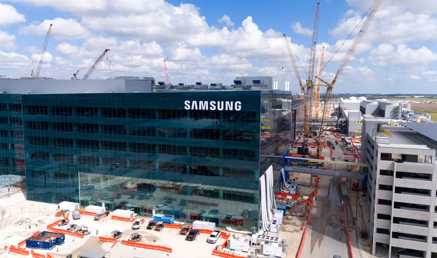
Samsung has reportedly resumed investment in its semiconductor fabrication project in Taylor, Texas following a major supply agreement with Tesla. The South Korean technology giant — which paused construction in September 2024 due to weak demand for foundry services — is now moving forward with renewed capital allocation, equipment procurement and phased hiring to bring the facility online for advanced 2nm production.
What changed: Tesla agreement sparks new momentum
Reports from Korean media indicate that a recent high-value contract with Elon Musk’s Tesla, covering 2nm-class chips, accelerated Samsung’s decision to reactivate development at the Taylor site. Samsung is allocating roughly $4 billion to resume construction and factory outfitting; part of that capital is being used to place equipment orders worth about four trillion won (approximately $2.87 billion). The company has also begun a targeted recruitment drive for engineering and operations staff, with two hiring waves planned for September and November.
Phased hiring and leadership
Sources close to the project say personnel selection is complete and deployment will follow the planned two-phase schedule. Until now, the Austin fab lead had been overseeing Taylor, but Samsung has named a dedicated head for the Taylor facility as the buildout ramps up — a sign the company expects significant, sustained production activity.
Product features: SF2P second-generation 2nm process
Samsung is preparing the Taylor plant for its SF2P technology, the company’s second-generation 2nm process node. While Samsung and other foundries do not publish all process parameters publicly, next-generation 2nm nodes typically emphasize the following product features:
- Higher transistor density for more performant system-on-chips (SoCs).
- Improved power efficiency enabling longer battery life in mobile and reduced energy use in data centers.
- Enhanced performance per watt for AI accelerators and vehicle compute modules.
- Support for heterogeneous integration and packaging for increased functionality per package.
These attributes make 2nm-class nodes attractive for demanding use cases such as electric vehicle (EV) systems, AI inference accelerators, high-end mobile SoCs and cloud-native processors.
Comparisons and market positioning
Samsung’s SF2P aims to compete with other advanced node offerings from global foundries. Compared with older nodes (5nm and 3nm), 2nm-class processes typically deliver marked improvements in power and density. In practical terms:
- Versus 3nm: Expect reduced power consumption and higher performance density, enabling more complex ML models on the same silicon budget.
- Versus legacy nodes (7nm+): 2nm yields substantial area savings and power reductions, making high-performance chips more cost-effective for space-constrained designs like EV compute stacks.
While exact performance comparisons depend on design, IP and packaging choices, having a U.S.-based 2nm-capable fab strengthens Samsung’s foundry proposition for customers wanting onshore manufacturing and supply-chain resilience.
Advantages and strategic relevance
Resuming the Taylor facility offers multiple advantages:
- Supply chain diversification: Adding advanced foundry capacity in the U.S. reduces logistical and geopolitical risk for global customers.
- Access for automotive and AI customers: Proximity to U.S. automakers and cloud providers enhances collaboration on customized nodes and qualification cycles.
- Economic and workforce impact: The project creates high-skill engineering jobs and supports partners in equipment and materials supply chains.
For Samsung, the Taylor investment helps secure long-term revenue from high-value customers such as Tesla and signals commitment to competing at the most advanced process nodes.
Use cases: who benefits from Taylor’s 2nm output?
The Taylor fab’s SF2P 2nm capacity is tailored to markets where performance per watt and integration density matter most:
- Automotive: EVs and autonomous driving systems require powerful, energy-efficient compute for perception and control.
- Artificial intelligence: Edge and datacenter inference accelerators benefit from 2nm’s improved performance density.
- Mobile and consumer SoCs: Premium smartphones and AR/VR devices can leverage reduced power draw for longer battery life.
- High-performance computing: Custom silicon for cloud providers and specialized compute tasks can use 2nm for performance advantages.
Market relevance: implications for the global chip industry
Samsung’s restart of Taylor underscores continued competition among global foundries to capture advanced-node demand. For the U.S., it supports semiconductor manufacturing capacity expansion and aligns with broader industry efforts to reshore advanced fab capabilities. For customers, a second U.S.-based 2nm-capable facility increases options for sourcing cutting-edge process technology and may reduce lead times compared with overseas-only manufacturing.
What to watch next
Key near-term developments to follow include: equipment delivery schedules, progress on facility construction milestones, the timeline for SF2P production ramp, and new customer signings beyond Tesla. How Samsung balances capacity allocation between mobile, automotive and AI workloads will shape the commercial success of the Taylor fab in a competitive foundry landscape.
Overall, Samsung’s renewed investment in Taylor marks an important step in bringing next-generation 2nm foundry capability to the U.S. market — a move with technical, economic and strategic implications for semiconductor design houses, automakers and cloud providers worldwide.
Source: sammobile
Leave a Comment