8 Minutes
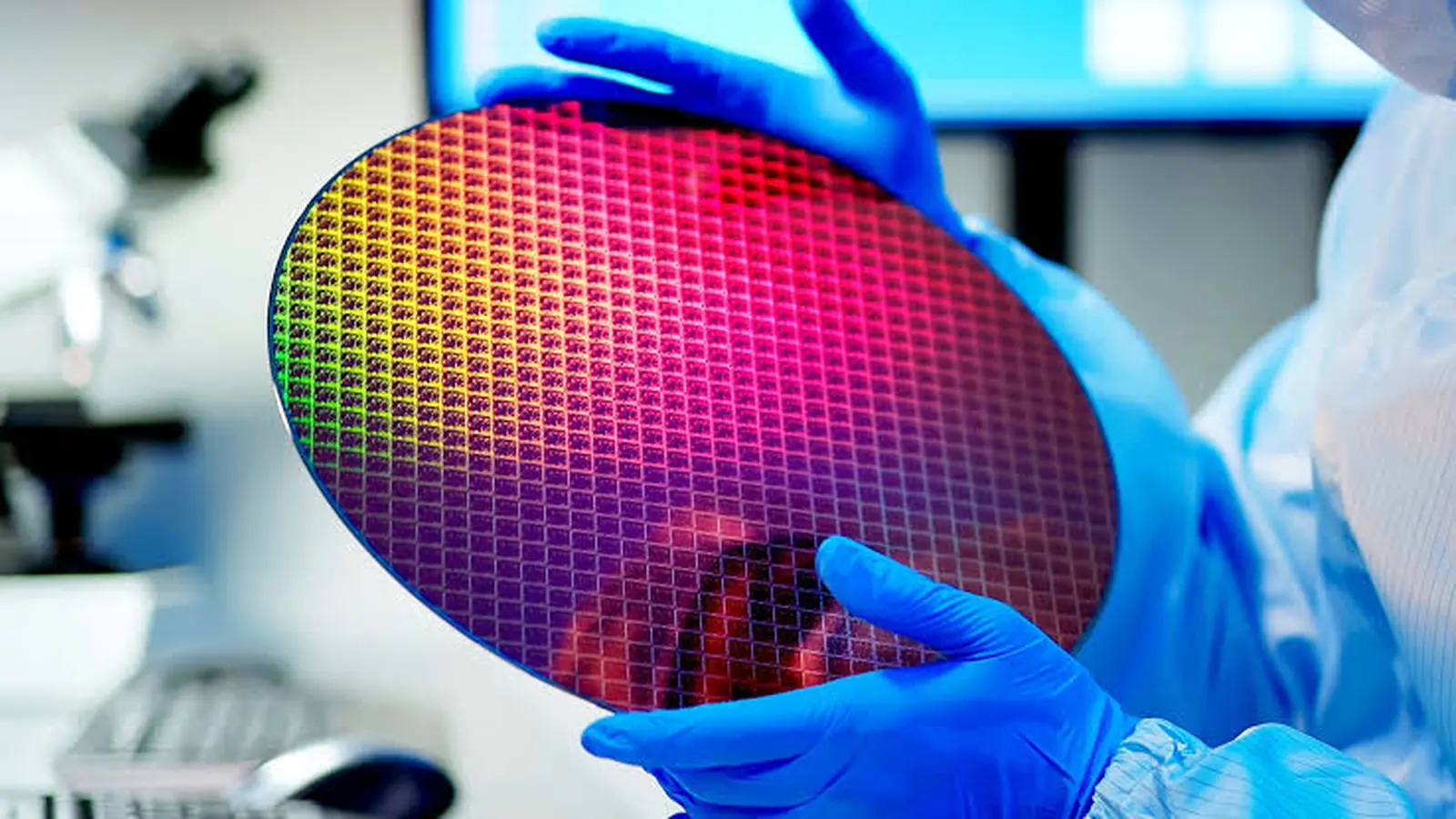
New electron-mediated entanglement in silicon
UNSW engineers report a major step toward scalable, silicon-based quantum computing: they have demonstrated controlled entanglement between the nuclear spins of two phosphorus atoms inside a silicon chip by using electrons as mediators. Published in Science (Sept. 18, 2025), the experiment shows that atomic nuclei can exchange quantum information at distances and on length scales compatible with modern semiconductor fabrication.
Artist’s impression of two nuclear spins, remotely entangled via the geometric gate applied via the electron
This achievement addresses a central trade-off in quantum hardware design. Nuclear spins are exceptionally well isolated from noise and can store quantum states (qubits) for tens of seconds, but that isolation makes it hard to couple many qubits together. The UNSW team used electron-mediated interactions to connect otherwise isolated nuclear-spin qubits while preserving their long coherence times — a combination that has been elusive until now.
Scientific background: nuclear spins, coherence and scale
Nuclear spins are a leading candidate for long-lived qubits. In silicon devices doped with phosphorus, each phosphorus nucleus carries a quantum spin that can represent a qubit. These nuclear-spin qubits are notable for extremely low decoherence: the group at UNSW previously recorded coherence times exceeding 30 seconds in silicon, and quantum logic fidelities better than 99% for single-qubit gates. Such performance makes nuclear spins attractive as memory elements in a quantum processor.
But strong isolation is a double-edged sword. To perform multi-qubit logic and generate entanglement — the nonclassical correlation that underpins quantum advantage — qubits must interact. Historically, nuclear spins were coupled by sharing the same electron wavefunction: one electron localized so it overlapped several adjacent nuclei. That approach can yield clear, high-fidelity interactions, but it is hard to scale because the electron’s spatial extent is limited and controlling many nuclei via a single electron complicates individual qubit addressing.
The UNSW advance tackles that scaling bottleneck by separating the roles of storage and interaction: nuclei remain highly isolated, while electrons act as controllable communication channels that can be moved, shaped and tuned using voltages and gate structures compatible with silicon technology.
Experiment: electron "telephones" and 20-nanometre separations
Device architecture and fabrication
The demonstrator device used phosphorus atoms precisely implanted in an ultra-pure silicon substrate and patterned with metal gates typical of advanced CMOS processing. The phosphorus implantation was performed by collaborators at the University of Melbourne, and the silicon substrate was supplied by partners at Keio University; the fabrication steps follow processes that are already standard in semiconductor research fabs.
How electrons mediate communication
Instead of forcing multiple nuclei to share a single tightly confined electron, the team coupled each nucleus to its own electron and then engineered an interaction between those electrons. Electrons in semiconductors are quantum objects that can spatially extend and interact with each other. By shaping the electron wavefunctions with gate voltages and applying a geometric control protocol (a geometric gate delivered via the electron degree of freedom), the researchers made the two electrons overlap or influence one another at a distance.
When each electron is directly coupled to a nucleus, an electron-to-electron interaction becomes an effective channel for nucleus-to-nucleus communication. In effect, the electrons function as controllable "telephones": the interior nuclear-spin environment remains quiet and well shielded, while electronic modes carry entangling interactions between remotely located nuclear qubits.
The nuclei in the experiment were separated by roughly 20 nanometres — about one-thousandth of the width of a human hair. While small in absolute terms, this spacing is comparable to feature sizes used in current commercial silicon transistors and well within the reach of modern lithography and implant placement techniques.
Key findings and implications for scalable quantum processors
The central result is the creation of entangled nuclear-spin states between two phosphorus nuclei at a 20 nm separation using electron-mediated geometric gates. This entanglement is an essential resource for quantum algorithms and error correction.
Because the nuclear qubits remain isolated for long periods, the approach preserves excellent quantum memory characteristics while enabling controlled two-qubit interactions when needed. The electrons act as fast, tunable mediators: they can be repositioned or reconfigured electrically, allowing interactions to be switched on and off dynamically. That level of control is crucial for scaling to the hundreds of thousands to millions of qubits envisioned for fault-tolerant quantum processors.
The experiment removes a major architectural constraint: nuclear qubits no longer need to share a single electron to interact. Instead, coupling can be established between independently controlled electron-nucleus units. This modularity maps well onto wafer-scale semiconductor workflows and suggests that the trillion-dollar semiconductor manufacturing base could be adapted to produce silicon quantum processors built from nuclear-spin building blocks.
Technical advantages and remaining challenges
Advantages:
- Long coherence times: nuclear spins provide robust quantum memory well suited to error-corrected architectures.
- Compatibility with silicon fabs: device dimensions (~20 nm) align with contemporary transistor feature sizes, easing integration.
- Electrical control of electrons: electrons are straightforward to move and shape electrostatically, enabling fast gating and selective coupling.
Challenges still to address include:
- Extending this two-qubit demonstration to many-qubit arrays and routing schemes for electron-mediated links.
- Maintaining low error rates in multi-qubit operations and integrating with readout and control electronics at scale.
- Managing cross-talk and calibration complexity as the number of electron-mediated links grows.
Related technologies and comparisons
Other qubit platforms — superconducting circuits, trapped ions, semiconductor quantum dots, and color centers in diamond — each balance speed, coherence and scalability differently. Superconducting qubits perform fast gates but require dilution refrigerators and face coherence limitations; trapped ions offer excellent coherence and high-fidelity gates but are more challenging to integrate at chip scale. The phosphorus-in-silicon nuclear-spin approach combines exceptional coherence with a clear path to CMOS-compatible fabrication, positioning it as a compelling option for quantum memory and processor backbones when combined with faster mediator qubits.
Because electrons can be shaped and relocated by gate voltages, hybrid architectures are also possible: fast electron-spin or quantum-dot qubits could perform high-speed logic while nuclear spins provide long-lived storage and error-corrected memory. The UNSW result makes these hybrid schemes more practical.
Expert Insight
Dr. Lian Park, a quantum hardware specialist (fictional), comments: "This experiment demonstrates a pragmatic route to scale: keep the best quantum memories quiet, and use mobile electronic modes as controlled links. The technical challenge ahead is engineering routing and error-correction layers that preserve coherence while supporting high-throughput entangling operations. The compatibility with standard silicon processing is a major advantage — it lets us borrow decades of industrial know-how to build quantum hardware."
Path forward and outlook
The UNSW team notes that the technique is robust and extensible. The two-electron demonstration can be generalized by adding more electrons or by elongating electron wavefunctions to couple nuclei over larger areas. Because electrons are easy to manipulate electrically, coupling strengths and durations can be tuned rapidly, enabling gate sequences required by quantum algorithms and error-correction codes.
Near-term goals include integrating more qubits into linear and two-dimensional arrays, demonstrating repeated high-fidelity entangling gates, and showing compatibility with multiplexed readout schemes. Longer-term objectives focus on assembling these building blocks into fault-tolerant modules that can be tiled on a wafer.
Conclusion
UNSW’s demonstration that electrons can mediate entanglement between nuclear spins at silicon-scaled distances is a meaningful technical advance for quantum computing. By combining the long coherence of nuclear-spin qubits with electrically controlled electron-mediated coupling, the researchers offer a blueprint for building quantum processors that are both high-performance and compatible with existing semiconductor manufacturing. The experiment narrows a major gap between laboratory demonstrations of exceptional qubit coherence and the practical engineering needed for large-scale quantum systems. Future work will focus on expanding the number of coupled qubits, reducing multi-qubit error rates and integrating these elements into architectures suitable for fault-tolerant quantum computation.
Source: sciencedaily
Leave a Comment