4 Minutes
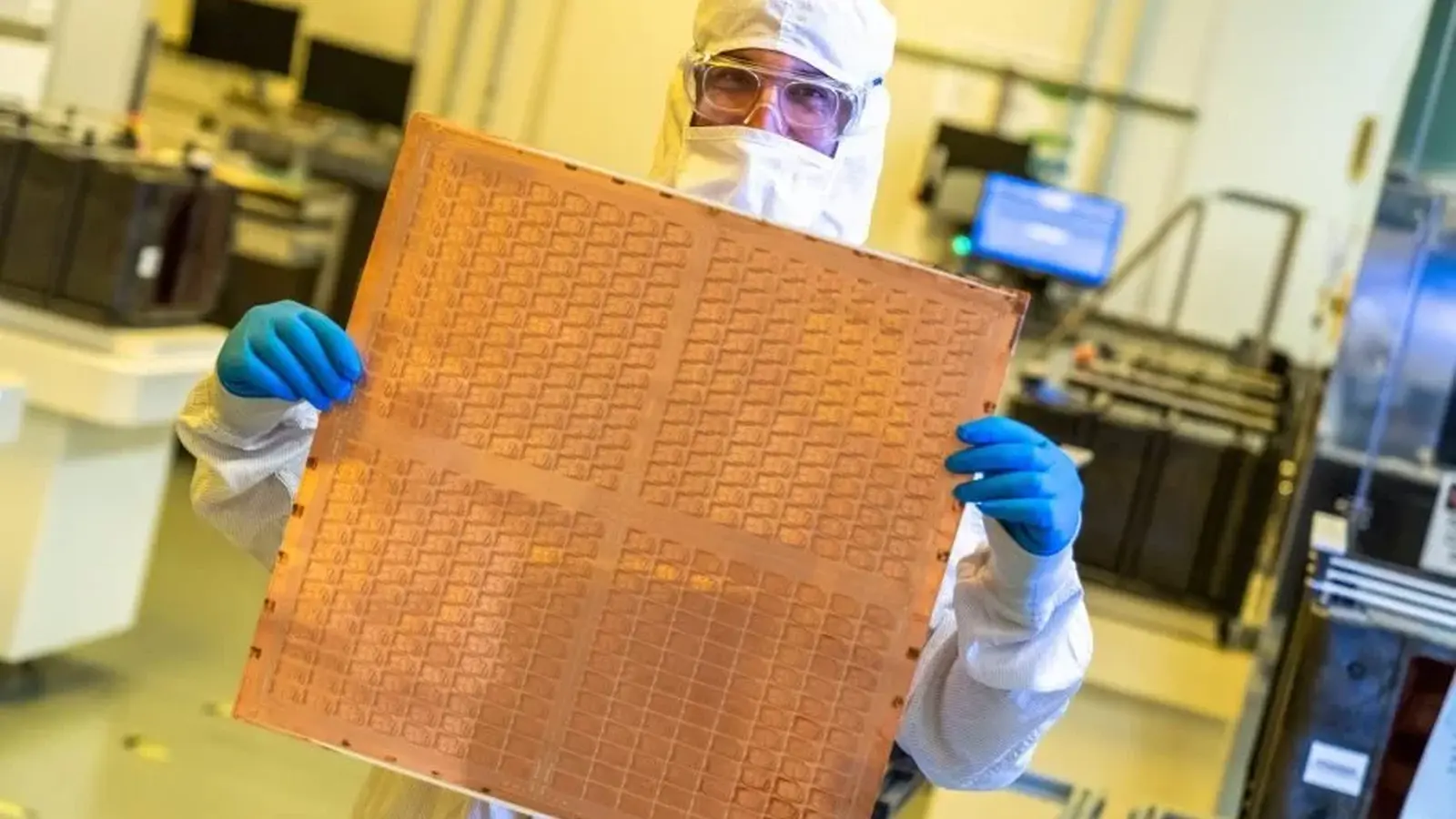
Imagine swapping the familiar circular silicon wafer for a slab the size of a laptop screen. It sounds like a small change. It isn’t. That shift — from round wafers to large rectangular panels — lies at the heart of TSMC’s push to tame the spiraling cost of high-performance chips.
TSMC is moving aggressively from CoWoS packaging to a panel-level approach called CoPoS, and glass-core substrates are central to the plan. CoWoS uses circular 300 mm wafers. CoPoS uses panels that can reach roughly 750 by 620 mm. Bigger real estate. Higher yield. Lower waste. The math is simple: more chips and memory modules fit per panel, which boosts material utilization and brings down per-unit surface cost by roughly 20 to 30 percent.

Why does this matter today? Because demand for AI accelerators and heavy-duty compute keeps exploding, and conventional packaging is running into physical and geometric limits. CoWoS’s round wafers create unavoidable material loss when you try to pack rectangular dies and memory stacks efficiently. Panels change the geometry of the problem, and glass replaces silicon as the substrate core to improve manufacturability at scale.
TSMC has already spun up a pilot CoPoS line and is racing the calendar. Internal plans point to pilot production around 2027 and a full ramp in 2028 for panel-level CoPoS wafers. Glass-core iterations are slated for broader adoption after 2030, with the company’s Arizona facility expected to play a significant role between 2029 and 2030. Those timelines align with rival moves; Intel has signaled similar ambitions for panel-level fan-out packaging from its Rio Rancho center, setting the stage for intense competition in next-gen substrate tech.
Partnerships matter here. TSMC is collaborating with Taiwanese firms like Ibiden and Innolux to develop a three-layer structure where a glass core sits between two ABF layers. That hybrid stack promises the thermal, mechanical, and manufacturing advantages needed to make CoPoS production reliable and cost-effective. The same glass-core approach is being evaluated for CoWoS variants, too, because the industry wants any route that improves yield and reduces cost.

TSMC estimates CoPoS with glass-core substrates can cut effective per-unit surface costs by about 20–30 percent, a boon for giant multi-die AI packages.
Technical shifts are spilling into product roadmaps. Reports suggest AMD will be an early adopter of panel-level fan-out packaging and TSMC’s 1.4 nm process for its Zen 7 CPUs. But the implications go beyond client CPUs and GPUs. Combining FOPLP and CoPoS opens doors for much larger, multi-chip modules tailored to datacenters and AI accelerators — markets that prize performance-per-watt and cost-per-TOPs above consumer price points.
There is a catch, naturally. Scaling panel-level processes at the precision and yield rates modern chips require is a heavy lift. Equipment suppliers need new tools. Process control must tighten. Supply chains must adapt to glass-core laminates at volume. Still, the payoff is compelling: fewer dead edges, more usable area, and a path to pack more compute into a given production footprint.
So when we talk about the next wave of semiconductor scaling, think less about transistor density alone and more about the platform those transistors sit on. Packaging is rewriting the rules of chip economics, and TSMC’s push to CoPoS with glass cores could be the start of a new chapter in how chips are made and deployed.
Leave a Comment