
3 Minutes
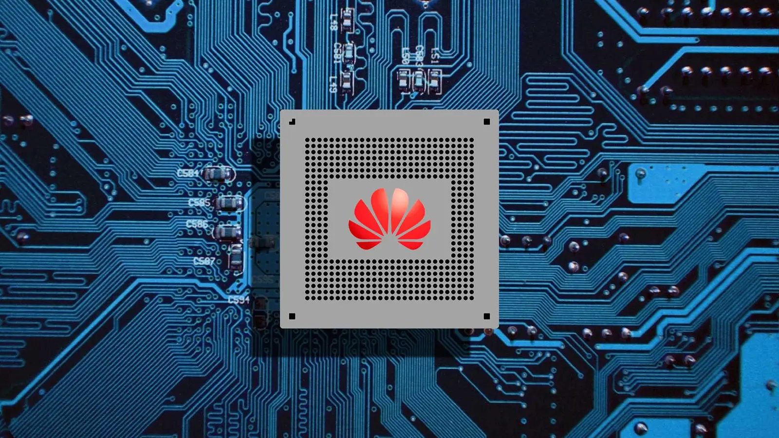
Imagine transistor progress measured by a clock instead of a ruler. That was the refrain in Shanghai this week as Huawei used its ISCAS keynote to sketch a future where chips scale along a timeline rather than only by geometry.
After decades of Moore's Law guiding the cadence of transistor shrinkage, the industry has run into stubborn walls: physics, cost and diminishing returns. Huawei argues those walls can be circumnavigated by changing the measuring stick. Enter the Tau (τ) Scaling Law — a time-centered formulation that reframes how performance gains are quantified and pursued.
Sounds bold. It is. But Huawei didn't just present a theory. Executives said the company has already mass-produced 381 chips designed under Tau principles, covering diverse industrial applications. That claim shifts the discussion from speculation to engineering practice, and invites the obvious question: can a new scaling paradigm move the entire ecosystem forward?

Part of Huawei's answer is an internal design approach it calls LogicFolding. At its core, LogicFolding compresses signal propagation delay and packs logic more efficiently without relying solely on geometric shrink. The result, according to Huawei engineers, is higher effective transistor density and faster signal paths — benefits that ripple through circuits, full systems and specialized chips alike.
The commercial debut won't wait for a decade. Huawei says next-generation Kirin smartphone chips slated for 2026 will be the first to use LogicFolding. The company expects those designs to reach consumers this fall, a timeline that will let the market test whether Tau and LogicFolding deliver real-world advantages over incumbent approaches.
Huawei projects that by 2031 its high-end chips will achieve transistor densities equivalent to 1.4nm nodes. That statement is provocative: it ties an abstract scaling law to a concrete manufacturing target. If validated, it would mark a major milestone in how the industry defines node progress — not just by nanometers on a chart but by effective performance and timing gains.
Practical hurdles remain, and Huawei didn't gloss over them. Manufacturing partners, lithography tools, materials science and EDA workflows must adapt. No single company can retool the ecosystem overnight. That's why Huawei leaned heavily on the language of collaboration during the presentation, calling for openness and cross-industry cooperation to navigate the next phase of semiconductor innovation.
Will the industry swap rulers for clocks? Watch for the Kirin launches this fall and the technical papers to follow. Those deliverables will say more than slogans, and they might just steer the conversation about what 'scaling' should really mean in the years ahead.










Leave a Comment
Comments
No comments yet. Be the first.