
4 Minutes
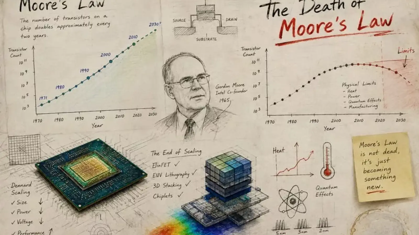
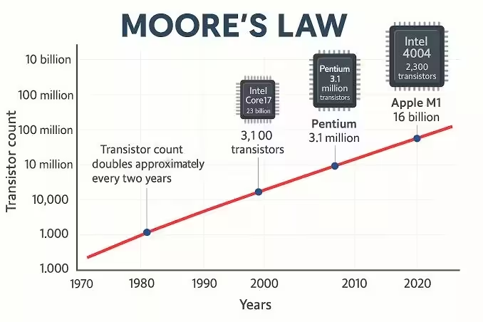
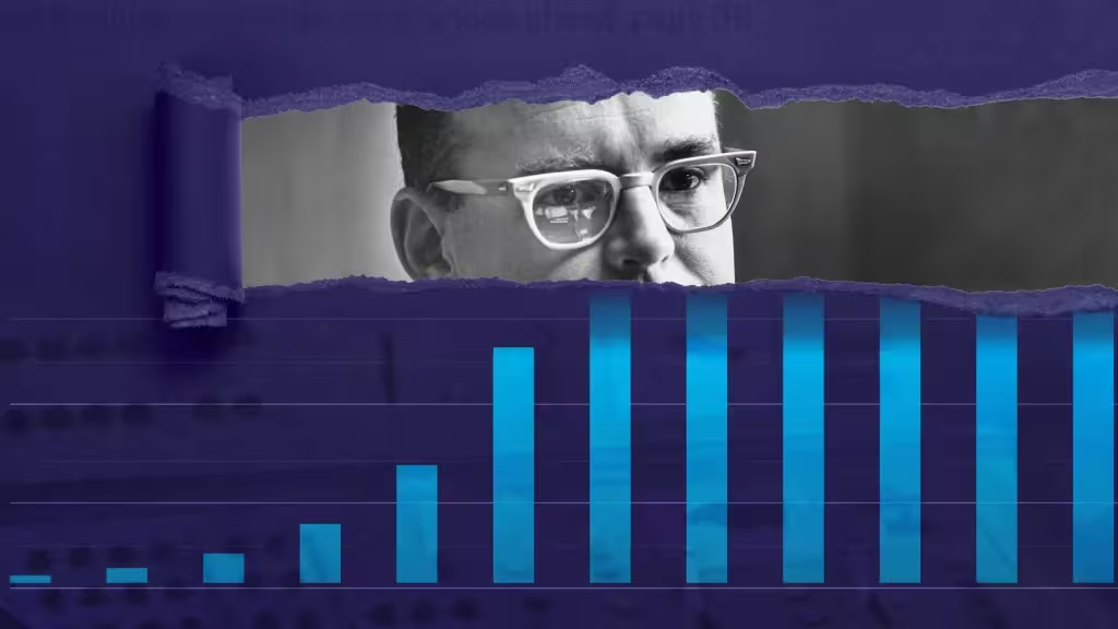
On a spring day in 1965 a short note by a 36-year-old engineer set a cadence for modern technology. Gordon Moore's observation — that transistor counts would roughly double every 18–24 months while costs fell — became less a prediction and more a promise. For decades that rhythm powered an era: room-sized mainframes gave way to pocket-sized computers with more processing muscle than the spacecraft that first reached the moon.
Promises, however, have an expiry tied to the laws of nature. Shrinking transistors worked wonders until their scales bumped up against atoms. Dennard scaling once guaranteed better performance and lower power as features shrank, but that rule broke down long before chips hit atomic dimensions. The gains that felt inevitable began to slow, then stall.
How and why did the sprint slow to a grind? Physics, blunt and uncompromising. Once gates on transistors are only a few nanometers wide — literally a handful of silicon atoms — electrons stop behaving like neat billiard balls. They behave like waves. They tunnel. A transistor meant to be off can leak current because an electron can 'tunnel' through what used to be an impenetrable barrier. Tiny leaks add up. Billions of leaking switches on a single die turn a clever processor into a compact heater.
Heat brought another limit: the thermal wall. Clock speeds climbed from single-digit gigahertz toward previously unthinkable numbers, but around 4 to 5 GHz the returns vanished. Crank the frequency and you don’t just compute faster; you cook the chip. That led to the curious and expensive phenomenon called dark silicon — large swaths of a chip that must remain powered down at any given moment to avoid meltdown. More transistors no longer meant more usable performance.

Engineers refused to accept defeat. They reshaped transistors in three dimensions. In 2011 the industry embraced FinFETs, a fin-like structure that lets the gate control the channel from multiple sides and rein in leakage. FinFETs bought the roadmap another decade, enabling 7 nm and 5 nm nodes. But as nodes crept toward 3 nm and below, even FinFETs faltered. The answer was a tighter embrace: GAAFETs, where the gate wraps fully around nanoribbons or nanosheets, squeezing every escape route shut. Building such atomic-scale sculptures is one of engineering's great feats.
Yet physics is only half the story. Economics wrote the other chapter. Photolithography at the cutting edge now depends on extreme ultraviolet tools — massive machines essentially impossible to build without enormous expertise. ASML in the Netherlands is the sole supplier of EUV steppers that can print 3 nm-class features. Each unit towers like a bus, contains more than a hundred thousand parts, and costs on the order of three hundred million dollars. A modern leading-edge fab? Expect price tags in the tens of billions. These numbers have reshaped the industry: a landscape that once hosted dozens of silicon makers has concentrated into a handful of giants.


So what happens when you can’t just make transistors tinier forever? You change the rules. The industry is shifting from monolithic, one-size-fits-all CPUs to heterogeneous systems and chiplet-based designs. Rather than forcing every function into a single die made on the same node, designers stitch together smaller tiles — chiplets — that can be manufactured using different processes and then integrated with advanced packaging. It’s pragmatic. It’s cheaper. It’s flexible.

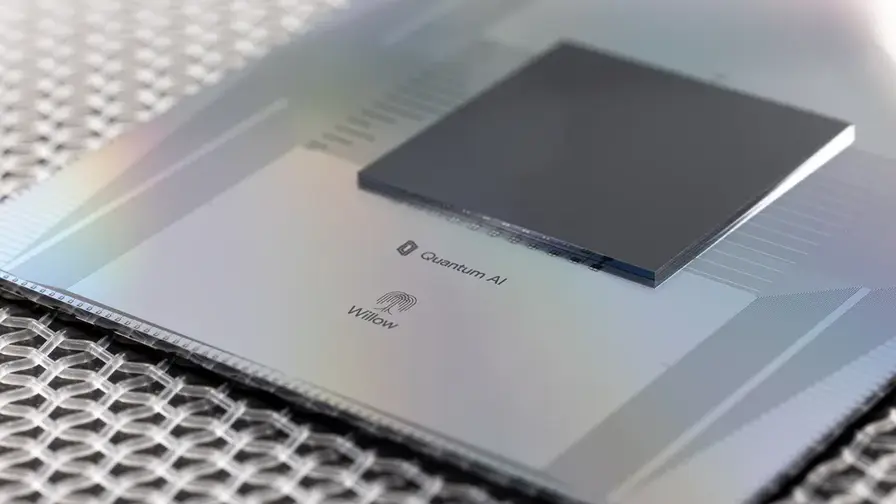
Specialized accelerators also have risen to prominence. GPUs, neural processing units, and domain-specific chips like Google’s TPUs or Apple’s M-series silicon show that raw transistor density isn’t the only path to performance. Offload the math to hardware built for that math, and efficiency shoots up. Photonics — using light instead of electrons for some communications and computing tasks — is gathering pace too, promising lower power for data movement. And at the far edge of possibility, quantum computers offer a radical, different model of computation rather than a mere miniaturization of existing ones.
Moore’s Law hasn’t died; it has been rerouted into smarter architectures, new materials, and system-level thinking.
The story of semiconductors has moved from a single metric — transistor density — to a broader portfolio of trade-offs: cost per function, energy per operation, and the ability to assemble heterogeneous pieces into cohesive systems. The future will be less about relentless shrink and more about clever composition: chiplets and 3D stacking, photonic links, specialized accelerators, and software that orchestrates diverse components efficiently.
Engineers are not surrendering to quantum limits. They’re redesigning the battlefield. When one door in physics closes, they smash through the wall to make a window. The next decade will look different than the last, but it will be no less inventive — and perhaps more interesting.

Leave a Comment
Comments (2)
Is this even true? ASML being the sole supplier feels risky, are there realistic alternatives or backup plans, curious...
wow this is wild! chips becoming tiny heaters, yet folks keep jury-rigging clever fixes... love the raw inventiveness