
3 Minutes
Intel has quietly moved the finish line forward. What was once penciled in for 2029 is now slated for high-volume manufacturing in 2028, and that change matters.
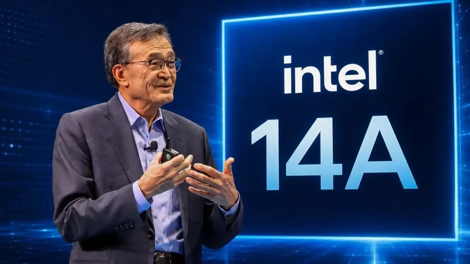
During its latest earnings call, CEO Lip-Bu Tan framed the 14A node as more than a roadmap milestone; he described it as a competitive lever for power efficiency, density, cost and timing. Short sentence. Big implication.
Behind that confidence sits tangible momentum. Intel’s foundry arm reported that Intel 7, Intel 3 and Intel 18A all surpassed internal volume targets last quarter. That performance wasn’t an accident. Better cycle times, higher wafer inventory and steady gains in yield pushed throughput up. The result: more chips out the door, and faster validation for customers.

18A in particular has seen a noticeable uptick in output, smoothing the way for upcoming products such as Panther Lake branded Core Ultra Series 3 and Wildcat Lake Core Series 3. Risk production for an 18A-P variant is already underway, which gives Intel practical lessons to apply to 14A development.
Intel now expects 14A high-volume manufacturing in 2028, with risk-production for internal products targeted in the second half of 2027.
What makes 14A noteworthy is not merely timing. Intel says this node surpasses 18A on both defect-density metrics and transistor performance, a rare step-change in a market where improvements are usually incremental. Engineers have delivered PDK 0.5 to partners, and PDK 0.9 is on track for October, paving the way for broader IP validation and ecosystem readiness.
That ecosystem work is busy. Intel is validating an IP portfolio for 14A and courting external customers while simultaneously prepping several internal designs for early adoption. Customers appear eager: multiple collaboration deals have been signed, though the marquee partners prefer to stay out of the spotlight until they are ready to unveil their silicon.

There’s a commercial logic behind the rush. High-volume manufacturing plans signal to potential foundry clients that Intel means business — that the process is mature enough to support production-grade chips and that internal products will demonstrate the node’s advantages first. Demonstration matters. Seeing a flagship device built on a new node lowers perceived risk for partners considering a move.
Intel didn’t stop at process announcements. The company also introduced ControlFlag, an automated tool aimed at catching coding errors. It’s a reminder that Intel’s push extends beyond transistor physics: software validation and developer tooling are part of the package when you ask customers to migrate complex chip designs to a new process.

Lip-Bu Tan framed the progress as disciplined execution. He said the team keeps raising internal targets and responding to issues as they emerge. That posture — incremental pressure, relentless problem-solving — is what has moved dates forward and production windows earlier than previously expected.
So what now? Watch PDK 0.9 in October, watch customer disclosures, and watch Intel’s internal parts that will act as proof points. If 14A hits the mark across power, density, cost and schedule, it could reshape conversations about where leading-edge chips are made.
And if not, the company will have learned a lot on the way. Either way, the foundry race just gained a new chapter—and the stakes are clear for partners deciding where to place their next bets.

Leave a Comment
Comments
No comments yet. Be the first.