
4 Minutes
Report explains why some Galaxy S26 models could get a price hike
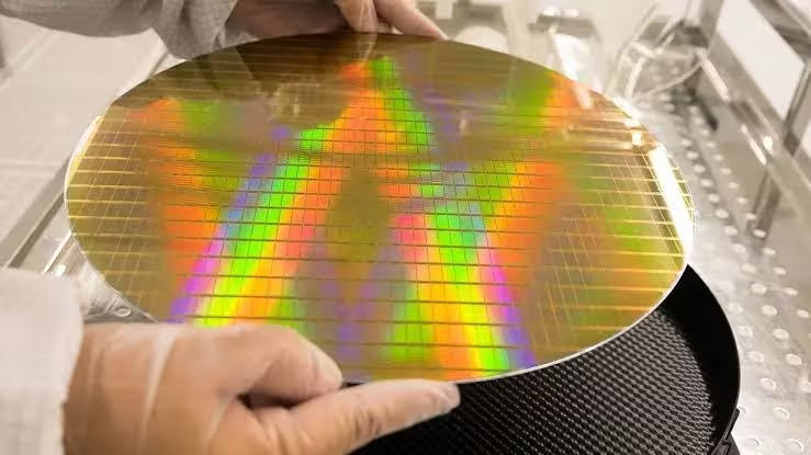
TSMC is currently producing advanced application processors (APs) on its third-generation 3nm process node (N3P). That same node is responsible for the Apple A19 and A19 Pro chips that power the iPhone 17 lineup, and it’s also being used to manufacture flagship APs like Qualcomm’s Snapdragon 8 Elite 5 and MediaTek’s Dimensity 9500.
TSMC hikes wafer prices for its 3nm N3P process
A China Times report says TSMC has raised silicon wafer prices for N3P, and that chipmakers are passing the cost along. According to the report, MediaTek is paying about 24% more and Qualcomm about 16% more for N3P wafers. The article doesn’t clarify whether those hikes are relative to TSMC’s earlier 3nm variant (N3E), which was used for the Snapdragon 8 Elite and Dimensity 9400.
Because Qualcomm and MediaTek must absorb higher wafer costs from TSMC, they will likely increase prices for their finished chips. That ripple effect could push OEMs to raise smartphone prices — which helps explain why some Galaxy S26 models may land with higher price tags next year. The vivo X300, expected to run on the Dimensity 9500, could face a similar bump.
If you’re wondering whether Apple also paid more for its 3nm wafers, the China Times report suggests it did. However, Apple designs its own APs and doesn’t pay a third-party chip designer; it deals directly with TSMC. That removes one layer of markup, so Apple’s supply‑chain cost structure differs from other phone brands that buy chips from Qualcomm or MediaTek.
The third-generation 3nm node is expected to deliver roughly a 5% performance uplift at the same power envelope, or a 5–10% power reduction at equivalent frequencies. As process nodes shrink, transistor sizes decrease and transistor density rises — measured in millions of transistors per square millimeter (MTr/mm²). Higher density typically translates to better performance and improved energy efficiency, making the density metric a key indicator of a chip’s capabilities.
Expect even higher chip pricing next year
Costs could climb again once TSMC ramps AP production on its 2nm node. Market speculation puts 2nm wafer prices as much as 50% higher than current 3nm rates. Apple has reportedly reserved roughly half of TSMC’s 2nm capacity, which may squeeze Qualcomm and MediaTek’s ability to secure ample production slots.
TSMC is said to target about 60,000 2nm wafers per month across four fabs. Early 2nm APs could show up first in premium handsets such as the Samsung Galaxy S26 Pro and Galaxy S26 Edge. Those models may use Samsung’s Exynos 2600 AP in many regions (excluding the U.S., Canada and China), produced by Samsung Foundry on its 2nm node.
Both Samsung Foundry and TSMC’s 2nm nodes will use Gate-All-Around (GAA) transistor architecture. GAA wraps the gate completely around the channel, minimizing leakage and boosting drive current — which yields better performance and lower power draw. Apple’s first 2nm iPhones, expected next year, should feature the A20-series APs.
Looking further ahead, TSMC plans mass production of a 1.4nm node in 2028 but will shift naming from nanometers to angstroms (Å). Under that scheme, 1.4nm becomes A14 (1 nm = 10 Å). Beyond A14, the industry may adopt new transistor architectures and alternative materials to sustain scaling and performance gains.
Source: phonearena
Leave a Comment