
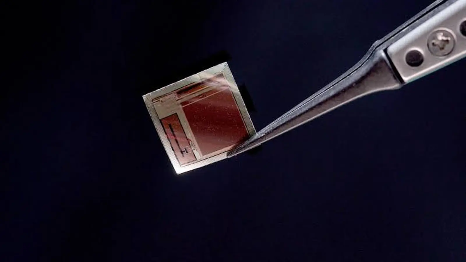
Imagine a transistor channel thinner than a single strand of DNA, yet still able to conduct and switch like the heart of a modern processor. Sounds like science fiction? It’s the very image researchers at National Yang Ming Chiao Tung University and TSMC are chasing — and inching toward reality.
The trouble has never been the channel alone. The real fight plays out at the razor-thin border where that atomically thin semiconductor meets its insulating gate. Make the dielectric too thin and the transistor behaves; make it too close to the channel and electrons scatter, performance collapses. The NYCU–TSMC team chose a different tack: don’t invent a new semiconductor. Redesign the interface.
They started with CVD-grown monolayer MoS2, a 0.7-nanometer-thick transition metal dichalcogenide that promises the thinness silicon cannot sustainably reach. Chemical vapor deposition matters: it produces continuous films over wafer-sized areas — essential for any path toward manufacturing, not just lab curiosities.

Why is the interface such a headache? MoS2 has almost no dangling bonds on its surface, so conventional oxide deposition struggles to form a uniform, defect-free film. The usual fixes — seed layers, surface treatments, or different oxide chemistries — helped but never delivered all three things at once: extremely small equivalent oxide thickness (EOT), tight gate control, and preserved carrier mobility.
What the team did feels elegant because it is small. They epitaxially deposited a single atomic layer of aluminum on the MoS2, then oxidized it into an about 0.42-nanometer-thick aluminum oxide buffer. On top of that they grew a high-κ hafnium oxide gate dielectric. The aluminum oxide acts like a microscopic foundation and a peacekeeper: it gives the hafnium oxide a smooth surface to grow on and it tames the electrical interactions that otherwise degrade the channel.
Engineering this atomic buffer produced a structure with an equivalent oxide thickness near one nanometer while preserving electron transport in monolayer MoS2.

How did the devices behave? Short-channel top-gate transistors with ~100 nm channels reached a peak transconductance of about 0.45 mS μm⁻¹, showed low leakage, and exhibited minimal hysteresis as gate voltage was swept back and forth. In plain language: the gate had strong control, the channel still carried current efficiently, and the devices were electrically stable during probing.
Those numbers are notable not because a single metric is world-beating, but because several historically conflicting properties were achieved together: near-1 nm dielectric scaling, strong electrostatic control, and retained carrier mobility — all on CVD-grown monolayers relevant to wafer-scale processing.
There are trade-offs remaining. Repeatability across full wafers, long-term reliability, and integration with standard CMOS processes still need work. But the result reframes the problem. At atomic thicknesses, the interface is not a mere seam; it becomes an active device element that can be engineered to steer electrons rather than scatter them. That shift in thinking — from swapping materials to sculpting their boundary — could open new design pathways for low-power logic and other advanced electronics as conventional silicon scaling slows.
Professor Wen-Hao Chang from NYCU emphasizes that the boundary between materials can be as influential as the materials themselves. Professor Tsung-En Lee adds that atomic-precision interface engineering gives designers degrees of freedom that changing a single material cannot. It’s a subtle pivot, but an important one.
The experiment also highlights a pragmatic advantage: using CVD-grown MoS2 means the demonstration is not limited to tiny exfoliated flakes. Growth techniques already exist for wafer-scale monolayers; the remaining challenge is marrying those films with reliable, repeatable interface engineering and processing compatible with industry tooling.
Think of it as tuning the joints instead of replacing the beams. The chip industry has long relied on material substitution and geometric scaling. As dimensions slip into the atomic realm, the seams—those interfaces a few atoms thick—will decide whether a promising material becomes a viable technology.
There’s plenty of engineering between this lab result and a commercial transistor, but the work points a clear direction: for atomically thin devices, mastery of interfaces may matter more than the search for a single miracle material. The next leap may come not from a new compound but from learning to layer the familiar ones with atomic care.


Leave a Comment
Comments (2)
Is this for real? wafer scale repeatability and CMOS integration sound like huge hurdles, if true...
Wow, atomic buffer idea is kinda poetic, tiny tweak big payoff? If that scales, low power chips could change everything... maybe.