
8 Minutes
A team of U.S. universities and a domestic foundry has unveiled a new monolithic 3D chip architecture that stacks memory and compute vertically, dramatically shortening data travel and promising major gains for artificial intelligence hardware. The prototype — fabricated at SkyWater Technology’s U.S. foundry — demonstrates the highest density of vertical wiring yet and shows clear, measurable performance advantages over conventional 2D designs.
Why stacking up changes everything
Modern AI systems demand massive amounts of data be shuttled between memory and processing units. Traditional chips place logic and memory side-by-side on a single plane, forcing data to travel along long, often congested routes. That bottleneck — widely known as the “memory wall” — limits how quickly a chip can feed its processors, even as those processors become faster and more numerous.
Monolithic 3D integration takes a different approach. Instead of spreading components across a flat surface, designers build many ultra-thin circuit layers directly on top of one another and connect them with dense vertical wiring. This architecture collapses the long pathways that slow data movement, enabling memory to sit right next to the compute elements that need it most. The result: far more efficient communication, higher throughput, and lower energy per operation.
From labs to a U.S. foundry: how they built the prototype
The project is a collaboration among researchers at Stanford University, Carnegie Mellon University, the University of Pennsylvania, MIT and SkyWater Technology — the largest U.S.-based pure-play semiconductor foundry. Unlike earlier 3D efforts that stack separately fabricated chips, this work uses a monolithic process: each new layer is fabricated directly on the previous layers in one continuous flow.
One of the technical hurdles for monolithic stacking is thermal budget — the maximum temperature a chip can tolerate without damaging layers already completed beneath it. The team used low-temperature processing steps that preserve existing circuits while allowing additional tiers to be deposited and patterned above. This tight thermal control enables layer-to-layer connections that are far smaller and denser than the coarse interposers used in conventional stacked assemblies.
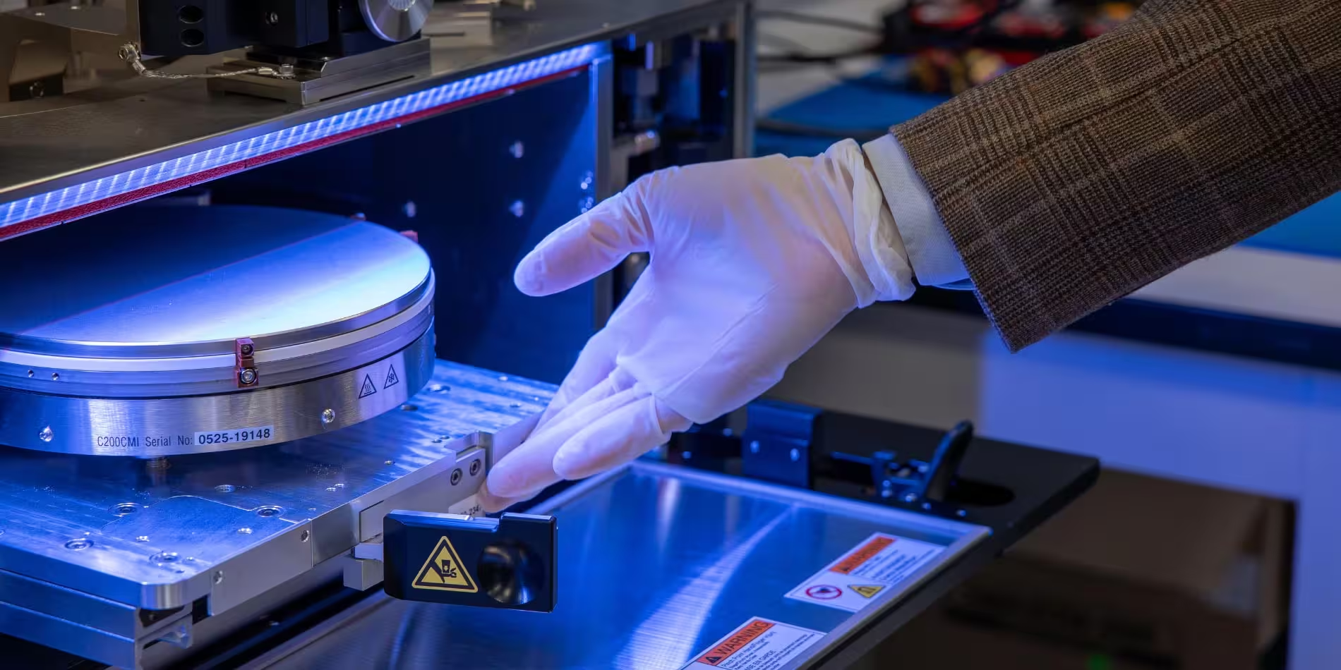
To test the new chips, the researchers used a special machine, like the one pictured here, to perform automated electrical characterization of the designs on a wafer of chips.
Completing fabrication inside SkyWater’s Minnesota foundry is more than a manufacturing milestone — it signals that advanced 3D chip architectures can be translated from academic prototypes into processes compatible with domestic commercial fabs. As Mark Nelson, vice president at SkyWater Technology, explained in discussions around the work, enabling commercial-scale production on U.S. soil is crucial for supply-chain resilience and national technology leadership.
Measured gains and simulated potential
Early hardware tests of the prototype reveal meaningful performance advantages. The first-generation device outperformed like-for-like 2D counterparts by roughly four times on select benchmarks. When the team ran simulations of taller designs — chips with more stacked tiers of memory and compute — they observed gains up to an order of magnitude (and in certain AI workloads, improvements as high as 12x).
Perhaps most compelling is the projected improvement to energy-delay product (EDP), a combined metric that balances speed and energy consumption. By dramatically shortening data paths and multiplying vertical interconnects, monolithic 3D chips can reduce the energy required per operation while increasing throughput. The researchers point to realistic paths toward 100–1,000x improvements in EDP compared with current 2D architectures, if taller stacks and optimized designs are realized.
Science background: the memory wall and the miniaturization limit
Two long-term trends have constrained chip performance. First, AI workloads require vast, fast-moving datasets. Second, the semiconductor industry’s traditional route to higher performance — shrinking transistor sizes and packing more devices onto a flat die — is reaching hard physical and economic limits, commonly called the “miniaturization wall.”
Stacking vertically addresses both constraints. Instead of only squeezing more transistors into the same plane, designers add more layers of functionality in the third dimension. Memory can be distributed throughout the stack, so compute cores have rapid, local access to the data they need. The architecture therefore attacks the memory wall directly, while offering a complementary path beyond simple transistor scaling.
Why U.S. domestic fabrication matters
Having the entire process run in a U.S. foundry carries strategic significance. The work demonstrates that advanced monolithic 3D integration is not just a laboratory curiosity but can be produced using manufacturing practices available within the United States. For national security, industrial competitiveness, and the growing demand for domestic AI hardware, that translation matters.
Beyond fabrication, there’s an educational and workforce angle. The shift to vertical integration will require engineers and technologists trained to design, test, and optimize 3D systems. The project’s collaborators emphasize training programs and multi-institution hubs that already support student involvement and cross-disciplinary research, helping prepare the next generation of chip designers for a vertically oriented hardware landscape.
Expert Insight
“Monolithic 3D integration represents a fundamental rethinking of how we architect compute systems,” says Dr. Leila Martinez, a systems architect at a U.S. aerospace research center. “By putting memory closer to where computation happens, you reduce both latency and energy use. For AI and space systems — where payload, power, and performance are tightly constrained — that can be transformative. The trick will be scaling manufacturing while keeping defect rates and thermal management under control.”
Her observation underscores two realities: the approach offers powerful efficiency gains, but it also raises new engineering constraints. Vertical stacks must manage heat dissipation across tiers, maintain yield at higher densities, and integrate with existing design and verification ecosystems.
Remaining challenges and research directions
Although the prototype demonstrates notable improvements, several technical hurdles remain before monolithic 3D chips become mainstream. Key challenges include:
- Thermal management: Heat generated deep within a stacked die must be removed without damaging sensitive layers.
- Yield and defects: Tighter integration means faults in a single tier can affect an entire chip; manufacturing processes need low defect densities to keep costs acceptable.
- Design tools and methodologies: Electronic design automation (EDA) flows and verification tools must evolve to handle three-dimensional floorplanning, routing, and timing analysis.
- Materials and interconnect reliability: Long-term stability of vertical vias and low-temperature deposited materials must be validated for commercial lifetimes.
Research groups are actively addressing these issues. Thermal simulation, new cooling strategies, error mitigation techniques, and advances in low-temperature processing are all part of ongoing work. Industry partners, government funding agencies, and cross-institutional hubs are supporting efforts to translate lab advances into reliable products.
What this means for AI, space, and beyond
For AI developers, tighter memory-compute integration can enable larger models to run more efficiently, reduce cloud operating costs, and permit more capable on-device inference for edge and mobile systems. In space and defense contexts, where power and volume are at a premium, monolithic 3D chips could allow more capable instrumentation and onboard processing within constrained mass and energy budgets.
The announcement also signals momentum for a broader domestic semiconductor ecosystem: universities training students, foundries adapting process flows, and federal and industrial funding aligned to reduce dependency on offshore manufacturing. Taken together, these elements point toward a future where U.S.-based research more readily transitions into production-ready hardware.
In short, the monolithic 3D chip prototype is an important step. It does not magically erase every engineering obstacle, but it provides a clear, manufacturable path to architectures that can break longstanding bottlenecks. For AI hardware designers, chipmakers, and policy makers, the work highlights a promising route to gain both performance and energy efficiency by rethinking the third dimension.
Source: scitechdaily
Comments
skyspin
Seen similar lab demos, promising but feels a bit overhyped. If fabs can keep defect rates low and cooling ok, could be huge. need real-world tests.
Tomas
Is this even true? 4x to 12x sounds wild, what about heat and yield in real chips, and long term reliability? curious.
mechbyte
Wow, that 3D stacking actually sounds massive for AI hw! If real at scale, latency and power would plummet, insane potential...
Leave a Comment